
Micro and Nanofabrication
Responsible researcher
Dr. Francisco Espinosa
Dr. Eider Berganza Eguiarte (RyC Track Researcher)
Research Facility´s Technical Responsible
Dr. Elias Saugar
Contact
+34 913349000 ext. 437013 / 132
+34 917165992 (direct number)
Location
ICMM-CSIC, Calle Sor Juana Inés de la Cruz, 3 28049 Madrid, España
Micro and nanofabrication room (009 – 011) 39 m2
- Plasma O2
- E-Beam Evaporator
- Sputtering
- Atomic Layer Deposition
- Wire Bonder
- Probe Station
Photolithography room (013) 19.82 m2 Controlled-environment cleanroom, classified as ISO 7 according to UNE-EN ISO 14644-1, with controlled airborne particle concentration.
- High-Resolution UV Lithography
- Nanoscribe Photonic Professional GT2 (PPGT2)
- Photolithography without mask
- Spin coater
- Fume hood
The Micro and Nanofabrication Clean Room is dedicated to the development of innovative technologies in the field of Materials Science, as well as other emerging Micro and Nanotechnologies. The facility is equipped with various coating and etching technologies, such as ALD, e-beam evaporation, sputtering, reactive ion etching (RIE), and oxygen plasma treatment. It also features a probe station for electrical measurements and a wire bonder for making microscopic connections using gold wire.
The Photolithography Clean Room is a controlled environment classified as ISO 7 according to UNE-EN ISO 14644-1, dedicated to the fabrication and processing of micro- and nanodevices using lithographic techniques. The facility is equipped with a high-resolution UV lithography system, the SÜSS MicroTec MJB4 Mask Aligner, a high-resolution 3D laser lithography system, the Nanoscribe Photonic Professional GT2 (PPGT2), and a maskless photolithography system. It also features a spin coater for substrate coating by centrifugation and a fume hood for the safe handling of chemicals and materials used in fabrication processes.
Equipment and services
Nanoscribe Photonic Professional GT2 (PPGT2)
The Nanoscribe PPGT2 is a high-resolution 3D lithography system based on two-photon polymerization (2PP), which allows the fabrication of complex micro- and nanostructures with sub-micron precision. It achieves lateral resolutions down to approximately 200 nm and vertical resolutions below approximately 500 nm, depending on process conditions and the resin used. The system has two objectives, 25× and 63×, and offers different writing modes, large writing fields, and high positioning precision.

Microlight 3D Smart Print UV
The Microlight 3D Smart Print UV is a versatile maskless lithography system that uses direct laser writing in the ultraviolet (UV) range. It enables fast and precise patterning, with typical lateral resolutions on the order of 1 µm, depending on the optical configuration and the resin used. The system has three objectives: 1×, 5×, and 10×.

Probe Station with Four Micromanipulators
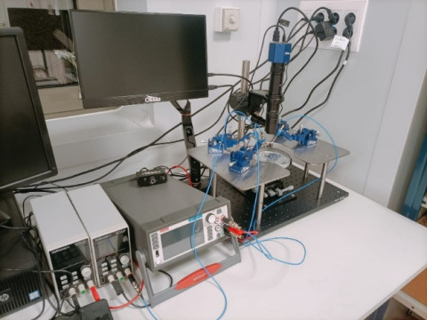
The Ossila probe station, equipped with four micromanipulators, provides a flexible platform for the electrical characterization of micro- and nanostructured devices. It allows precise positioning of up to four probes to perform current-voltage (I-V) curve, output curve, and transfer curve measurements.
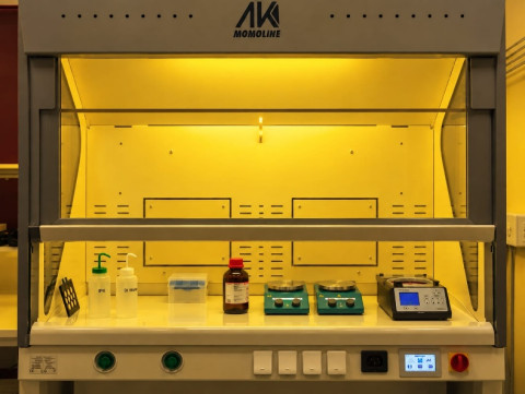
Ossila spin coater and fume hood
Fume hood for the safe handling of chemical products and processes that may generate vapors, gases, or particles, through controlled air extraction.
Deposition of uniform material layers on a substrate by spin coating. The maximum speed reached is 6000 rpm.
High-Resolution UV Lithography. (SÜSS MicroTec MJB4 Mask Aligner)
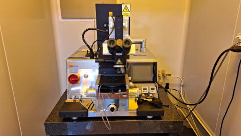
The MJB4 Mask Aligner offers high-precision mask alignment and high-resolution printing capability in the submicron range (~1 µm). It is equipped with a WEC head system that allows reaching the parallelism between substrate and mask with a micrometric precision.
Wafer Size 1 up to 100 mm / 4" (round)
Max. Substrate Size 100 x 100 mm
Contact: soft, hard, vacuum, soft vacuum
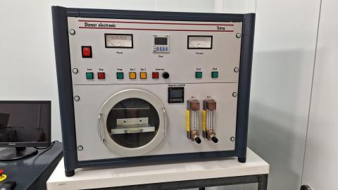
Low – pressure Plasma System. (Tetra Diener Electronic)
Removal or cleaning of organic materials from a substrate using oxygen plasma. This process is also used for material treatment.
Power: 200W (at 40Hz)
Base Pressure: 0.6 mbar
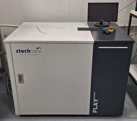
Atomic Layer Deposition. (CTECHnano Coating Technologies, Play Series
ALD has a cylindrical-shaped chamber, designed to ensure a consistent flow. It is highly versatile and can handle a wide variety of substrates and materials for deposition.
Precursors system with 4 lines.
Temperature Range: 0-200ºC (resolution 1ºC).
Control system: gas flow, temperatures, pressure, and valves.
Base Pressure: 10-3 mbar
E-Beam Evaporator. (EVM-6 Ferrotec)
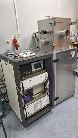
The electron beam evaporator is specifically designed to perform metal coatings with a variety of materials (Au, Ti, Cr, Pt, Ni...) in high vacuum.
Power: 6KW
Acceleration Voltage: 4-10 KV
Max. Filament current 50A
Spot Size Diameter <3 mm
Max. Evaporation Rate: 12.000 Å /min
Base Pressure: 10-7 mbar
Sputtering
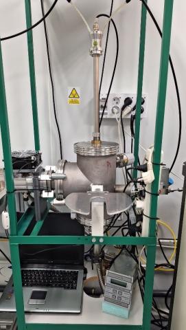
Sputtering is used for the controlled growth of nanometric thin films.
Wafer Size 1 up to 100 mm / 4" (round)
Max. power, watts DC/ RF: 600 W DC / 400 W RF
Max. voltage DC: 1000 V
Max. current DC: 5 A
Base Pressure: 10-5 mbar
Allowed samples
A variety of substrates and films can be used for the available Clean Room technologies, including Si, SiC, pyrex, 2D materials, etc.
Industrial Application Sectors
Electronics and Microelectronics, Aerospace and Automotive, Energy and Environment, Medicine and Biotechnology



Instituto de Ciencia de Materiales de Madrid (ICMM)
Sor Juana Ines de la Cruz, 3
Cantoblanco, 28049
Madrid, España
Telephone: (+34) 91 334 90 00
Email: @email
Communication Office: @email

Acknowledge the Severo Ochoa Centres of Excellence program through Grant CEX2024-001445-S/ financiado por MICIU/AEI / 10.13039/501100011033

Contacto | Accesibilidad | Aviso legal | Política de Cookies | Protección de datos