
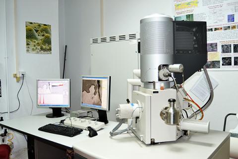
Microscopía electrónica de barrido de emisión de campo (FE-SEM)
Científicos responsables
Dr. Pilar Aranda (Investigadora Científica)
Dr. Miguel A. Camblor (Profesor de Investigación)
Personal técnico
Ismael Ballesteros (Ayudante de Investigación CSIC)
Andrea Rivas Garrido (Personal de apoyo)
Contacto
+34 913349000 ext. 437386
+34 91766520 (número directo)
Localización
Lab S37 (sótano)
Medidas
- Imágenes de alta resolución con información topográfica de la superficie, incluyendo visionado en sección transversal.
- Microanálisis químico cuantitativo mediante Espectroscopia de Energía Dispersiva (EDS). Mapeado de elementos químicos.
Equipo
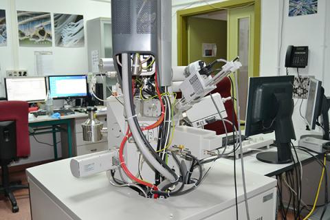
- Microscopio electrónico de barrido NanoSEM 230 de la marca FEI con cañón de emisión de campo tipo Schottky que permite la visualización de muestras a alto (HV) y bajo vacío (LV) (< 200 Pa) a potencial variable (50 V a 30 kV) y con la posibilidad de decelerar el haz de electrones. No se requiere metalización previa ni siquiera para muestras no conductoras utilizando la opción de bajo vacío.
El equipo incorpora varios detectores: electrones secundarios (SE) Everhart-Thornley para HV (SED), SE de bajo vacío (LVD), a través de la lente SE (TLD), electrones retrodispersados (BSE), a través de la lente (TLD-BSE), detector SED de ultra alta resolución en bajo vacío (Helix) así como un detector de nueva generación para la obtención de imágenes de alto contraste a bajos potenciales tanto en HV como en LV combinando los detectores SE y BSE (detector vCD). - Análisis químico cuantitativo con un detector de Espectroscopía de Energía Dispersiva (EDS) de nueva generación (Genesis XM2i de la marca EDAX Inc.) que permite la identificación de elementos con número atómico ≥ 5 (Boro) y resolución hasta 133 eV. También es posible la obtención de imágenes por elementos (mapeado químico elemental).
- Disponemos de portamuestras de diferentes tipos, incluidos portas especiales para vistas transversales.
Muestras permitidas
Cualquier tipo de muestra de un tamaño lo suficientemente pequeño como para entrar en la cámara del microscopio (<10 cm). Las muestras deben estar y permanecer completamente secas y deben ser estables bajo el haz de electrones. Normalmente, no se requiere metalización si se trabaja a bajo voltaje con el detector vCD mencionado.
Mantenimiento
Semanalmente se realizan una serie de ajustes y calibraciones conforme a las especificaciones del fabricante del equipo. Estas incluyen el alineamiento del haz de electrones y de las lentes, modulación del foco, alineación del corrector de astigmatismo, corrección de "image shift", y calibración de crossover. Estos procedimientos están igualmente documentados en el manual del equipo.


ICMM
Sor Juana Ines de la Cruz, 3
Cantoblanco, 28049
Madrid, España
Teléfono: (+34) 91 334 90 00
Email: @email
Oficina de Comunicación/Prensa: @email

Acknowledge the Severo Ochoa Centres of Excellence program through Grant CEX2024-001445-S/ financiado por MICIU/AEI / 10.13039/501100011033

Contacto | Accesibilidad | Aviso legal | Política de Cookies | Protección de datos