
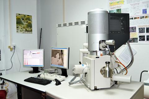
Field-Emission Scanning Electron Microscopy (FE-SEM)
Scientists in Charge
Dr. Pilar Aranda (Senior Scientist)
Dr. Miguel A. Camblor (Research Professor)
Technician
Ismael Ballesteros (Lab Technician)
Andrea Rivas Garrido (Research Facility´s staff)
Contact
+34 913349000 ext. 437386
+34 91766520 (direct number)
Location
Lab S37 (basement)
Measurements
- High-resolution images with surface topography information.
- Quantitative chemical microanalysis by Energy Dispersive Spectroscopy (EDS). Mapping
Equipment
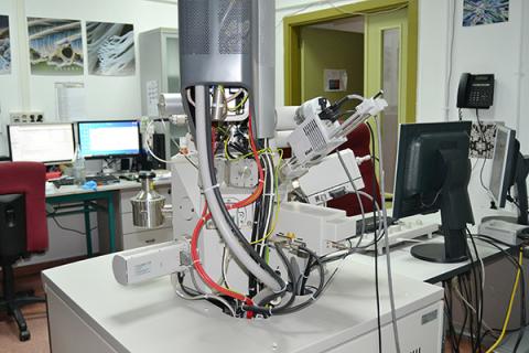
- FEI Nova NanoSEM 230 microscope with a Schottky field-emission gun that allows visualization of samples at high (HV) and low (LV) vacuum (< 200 Pa) at variable potential (50 V to 30 kV) and with the possibility of decelerating the electron beam. Previous metalization is not required even for non-conductive samples using the low-vacuum option. The equipment incorporates several detectors: secondary electrons (SE) Everhart-Thornley for HV (SED), low vacuum SE (LVD), through the lens SE (TLD), backscatter electrons (BSE), through the lens (TLD-BSE), ultrahigh resolution low vacuum SED (Helix) as well as a new generation detector for high contrast imaging at low potentials in both HV and LV combining SE and BSE (vCD).
- Quantitative chemical analysis with a new generation EDX detector (EDAX Genesis XM2i) that allows identification of elements with atomic number ≥ 5 (Boro) and resolution till 133 eV. Imaging by element is also possible (chemical mapping).
- There are sample holders of different kinds, including special ones for cross-sectional views.
Allowed samples
Any kind of samples of a size small enough to enter into the microscope chamber (<10cm). The samples must be and remain completely dry and must be stable under the electron beam. Typically, no metallization is required if working at low voltage with the vCD detector.
Maintenance
A series of adjustments and calibrations are performed weekly in accordance with the equipment manufacturer's specifications. These include electron beam and lens alignment, focus modulation, astigmatism corrector alignment, image shift correction and crossover calibration. These procedures are also documented in the equipment manual.


Instituto de Ciencia de Materiales de Madrid (ICMM)
Sor Juana Ines de la Cruz, 3
Cantoblanco, 28049
Madrid, España
Telephone: (+34) 91 334 90 00
Email: @email
Communication Office: @email

Acknowledge the Severo Ochoa Centres of Excellence program through Grant CEX2024-001445-S/ financiado por MICIU/AEI / 10.13039/501100011033

Contacto | Accesibilidad | Aviso legal | Política de Cookies | Protección de datos