
Andrés Castellanos-Gómez: "Looking at the right questions is what distinguishes a good researcher from a less good one"
He is member of the 2D Foundry group at ICMM. The scientist has received two prestigious awards this year.
 The years never pass the same for everyone, that's clear. But perhaps it can be said, with little margin for error, that 2022 has been the year of Andrés Castellanos Gómez. He has won one of the most relevant awards in science in Spain: the National Award for Young Researchers, awarded by the Ministry of Science. He has also received the Miguel Catalán sub-40 award, from the Community of Madrid, for his scientific contributions.
The researcher at the Institute of Materials Science of Madrid (ICMM), CSIC, has spent the last months of the year getting excited when thinking about these recognitions. He insists that his work is thanks to all those who trusted and trust him: his team now, full of young enthusiasts for two-dimensional materials; but also his mentors and those who welcomed him at the Higher Council for Scientific Research when he arrived “without sponsors”.
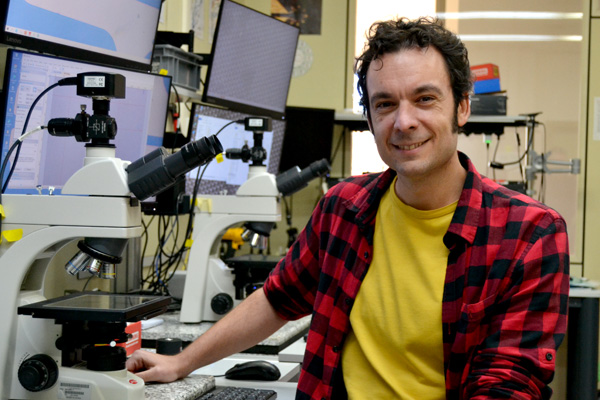
He studied Physics at the Complutense University, received his Ph.D. from the Autonomous University of Madrid, and went through Groningen and Delft (The Netherlands) before returning to Spain, where he relapsed at IMDEA Nanociencia before getting a place at ICMM. Here he talks about his work and how he sees science, always insisting on fellowship and fun as a basis for research.
The National Award highlights how your research "explores new materials of atomic thickness and studies their mechanical, electrical, and optical properties with a special interest in the application of these materials in nanomechanical and optoelectronic devices." What new materials are those?
Since 2004, when graphene was isolated, there has been a lot of work on it. My research has been based on materials that are very similar to graphene but have mostly semiconductor properties. They are analogous, from a structural point of view, to graphene: they are materials with very strong layers and bonds, which do not have unpaired out-of-plane bonds.
What is an unpaired link?
When an atom has a penchant for trapping electrons from another nearby atom. In some materials, it happens that when you exfoliate them, the atoms on that surface are left wanting to find another atom to share electrons. In the case of van der Waals materials, this does not happen: when you exfoliate them, the surface is completely passive, and atomically smooth, and the atoms do not have that desire to share electrons with others; They are, let's say, comfortable.
An example of those materials?
Graphite forms those layers that can be easily exfoliated. We work with semiconductors and a typical example is molybdenum disulfide, which is found in a mineral called molybdenite.
To continue in this first approach to the definition given by the national award of your work, now talk about nanomechanical and optoelectronic devices. What are nanomechanical devices?
They are electronic devices in which certain types of information are stored in mechanical degrees of freedom. Normally they are mechanical resonators in which one uses the different resonant frequencies of the material to store some type of information. It can be used as a memory or, for example, as a filter, a system that, having a well-defined resonance, allows lower frequencies to pass but does not allow higher frequencies to pass.
What could be achieved with this?
It is used for many things. These systems resonate at frequencies between one megahertz and one gigahertz. It is a super important frequency range for any electronic device. Mobile phones, for example, have radio frequency filters that are around ten megahertz, and they are very bulky filters. Much of the weight of a mobile phone is the megahertz filters. So if you could make those filters using a mechanical nanoresonator you could reduce the size of the phone a lot.
Another thing we were interested in at the time [during his time in the Netherlands] was quantum computing units, qubits. Solid-state qubits have a decoherence problem: they can perform quantum computing operations but that information is diluted over time, and the quality of the storage is lost. What we were trying to do at that time is to couple these cubits with mechanical resonators, to store the information that is generated in a cubit inside a mechanical resonator, as RAM memory, to later be able to use it in another subsequent operation.
You talk about what you wanted to do, but now your work has evolved
Since I returned to Spain I have focused more on optoelectronics, on the manufacture of photodetectors with these two-dimensional materials.
What are we talking about when we talk about optoelectronics or photodetectors?
Any light sensor is a photodetector. For example, cameras are an array of a bunch of photodetectors. We want to make them with these materials that are atomically thin. The first thing we do is build simple photodetectors that allow us to learn things about materials. We use the photodetector as a tool to study materials.
Another thing that I have been interested in recent years is in modifying the properties of these materials through mechanical deformation. Torture our crystals a bit so that they change their electronic and optical properties. So by coordinating these two actions together, we have the idea of making adaptive photodetectors. The classic example of what an adaptive photodetector is is the eye: you walk into a brightly lit room and the human eye has a certain spectral response and responsivity, but when you walk into a dark room the response of the eye changes. The idea we have is to make a photodetector that copies the operation of the human eye: we apply a mechanical deformation to spectrally shift this and raise or lower the responsivity.
Ok, we understand that it is with the human-eye example. Now, what would this do?
For example, to have the same camera that detects infrared at night and visible light during the day, because now this is done with two different cameras. We want the detector to be sensitive to different wavelengths: so that we can have spectral information in each pixel of the image, which has many applications in industry (food, above all). And from there you can imagine any daily scenario: for example, I always think about when you put sunscreen on the children, and you always doubt if there is a lack of space (laughs). If you had a hyper-spectral camera you could see if that piece was missing.
Also now your work is going towards non-polluting materials, how are you working here?
For a couple of years, we have started to integrate semiconductor van der Waals materials into biodegradable substrates. Instead of integrating our devices on silicon wafers, which is the standard, we are manufacturing them on substrates of paper, potato starch, and egg albumen... we try to combine other materials to be able to make devices that are biodegradable or that leave small traces of Van der Waals materials, which are non-polluting.
How is this process going?
Good. Until now I think that electronics on paper was dominated by people with a more chemical background and we are taking a slightly different view. I think we are providing new things in the field. And we are having a great time. We are learning a lot of new things. I am evolving towards a more applied profile and I feel quite comfortable with that.
When working with materials that come from nature, it must not be forgotten that nature is also finite. For example, when you work with paper, what do you use?
We use printer paper, but we have also used brown paper. To a large extent, virtually all cellulose substrates can be applied to the type of devices we develop. Maybe there are some performance differences, but I don't think it's very remarkable. From an environmental point of view, at least in Europe, the bins are highly controlled. No more trees are felled than are planted. Another thing is in other countries, but in Europe, that is very controlled.
You even work with toilet paper, which is a material that practically dissolves in contact with water. How do you deal with these difficulties?
It depends on the type of application one wants. The toilet paper thing was a proof of concept to start working on devices that are soluble in water. We are working with papers that dissolve in water because, in some applications, one wants the degradation of the device to happen very quickly. We look for this in disposable applications, for example, for biomedical use. If instead of just throwing away the device after using it, one can downgrade it directly, then you eliminate the problem of e-waste, which is the biggest problem that motivates us to work on paper electronics.
Where is your research going? Any new ideas?
It's hard to know. In research one always finds things that you did not expect, otherwise, it would be very boring.
Have you considered, years ago, the implementation of electronic devices on paper or potatoes?
No. What I did have in mind more or less from a vital point of view is that I wanted to transition towards more applied research. I did know that I have always been a very pragmatic person, but this is something that you allow yourself to do when you already have a fixed position when you can change the research topic in a more comfortable way.
Why?
When you are looking for your future, and your permanence in the research system, you have to have results, and radically changing your research topic entails a certain dry period.
Of course, in the end, it is the measure way... But now they continue to measure you by results.
Yes. Right now the evaluations have an impact on the funding I have to do science, but they do not have an impact on having a salary at the end of the month. It is a different level. You can afford to take those risks: in the worst case you get fewer projects, but it's a risk you can take. It may happen that you make a mistake, or that the topic is not good, but you can go back. There is always the researcher's ability to look for the right questions: many questions arise along the way, and looking at the right ones is what distinguishes a good researcher from a less good one.
In your group, you create your own machinery due to the lack of previous technology in the area. This in the end is another branch of research
Yes. Ultimately it is a personal decision. One can do research using only exclusively commercial devices. Also one can do research only with home appliances. We are somewhere in between for practicality. I like experimental setups that require little investment from an economic and time point of view, and that is easy to use. I believe that providing a community with the right tools makes that community grow. We always think that everyone does research at places like Stanford or MIT, but there are many more places doing science with more limited means. The fact of being able to provide certain tools helps the field a lot.
When you build your devices, you make them available to the scientific community
Yes, we publish it in the open. We usually publish articles in which we describe the assemblies with all kinds of details
And this is with the aim that people can replicate it
Clear. In fact, we have many visitors every year who come motivated by this. Maybe they've seen the post, they want to replicate this in their lab and they come in for a short visit to see exactly how it's set up and we give them a little training. Then they go back to their place of origin and make out.
Any specific case?
I was very excited about a student from Iran who spent six months with us. He is now back at Kurdistan University and has set up a small laboratory for optoelectronic devices.
The scientific community has this duality: on the one hand, you have to work as a team but then it is very competitive
I don't know... I think it's like a competitive sport. You're training with your teammate every day, but then you throw yourself in a pool next to him to see if you can beat him, and nothing happens. I guess that's why I see it naturally.
Instituto de Ciencia de Materiales de Madrid (ICMM)
Sor Juana Ines de la Cruz, 3
Cantoblanco, 28049
Madrid, España
Telephone: (+34) 91 334 90 00
Email: @email
Communication Office: @email

Acknowledge the Severo Ochoa Centres of Excellence program through Grant CEX2024-001445-S/ financiado por MICIU/AEI / 10.13039/501100011033

Contacto | Accesibilidad | Aviso legal | Política de Cookies | Protección de datos