
ICMM-CSIC researchers create a cost-effective technique to scale up the production of nanolayers of materials like graphene
Researchers at the Materials Science Institute of Madrid (ICMM-CSIC) have developed a novel mechanical exfoliation technique to obtain more and better nanolayers of van der Waals materials (those with a layered structure, like graphene) in a much more cost-effective way. The results of their work have just been published in the journal Small Methods.
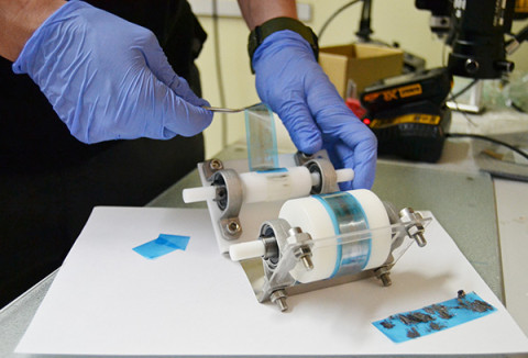
Until now, the mechanical exfoliation used to obtain layers of these materials involved using adhesive tape on the material to be exfoliated. When the tape is separated from the material, tiny layers adhere to it, which possess the specific properties sought after in each material. However, while this method is cost-effective and provides high-quality flakes, it is not as scalable as others. To address this, a roller system with opposing cylinders made of a polymer (polyoxymethylene) has been designed.
The rollers are covered with adhesive tape, and the material to be exfoliated is placed on them. When both cylinders rotate, they touch each other while turning, replicating on a larger scale the adhering/peeling process performed in manual mechanical exfoliation. "At the end of the process, the adhesive tape is completely covered with graphene, molybdenum disulfide, or any other layered material," explains Carmen Munuera, a researcher at ICMM-CSIC and one of the authors of the study.
To prevent the rollers from always touching at the same point, they were designed with diameters corresponding to large prime numbers, ensuring "that many revolutions are required before the cylinders return to their initial relative alignment," notes Andrés Castellanos-Gómez, another scientist from ICMM-CSIC and the lead author of the study. Thanks to this, the material is evenly distributed on the adhesive tape.
In this way, they have designed a device that is not only versatile because it can be used with different two-dimensional materials, but also provides optimal results (the layers have a high aspect ratio by achieving a good lateral size), and the material transfer is straightforward. "With our method, we have achieved a remarkable balance between cost, scalability, and performance," highlights Munuera, pointing out that, since the technique does not involve solvents, it also leaves no residues between the layers, "which would have a negative impact on factors like conductivity."
The equipment is relatively small, which allows them to work in confined spaces, necessary for materials that degrade under ambient conditions. Furthermore, the researchers have shared the blueprints of their invention in the paper itself so that any other laboratory can replicate and work with it.
"This method offers opportunities for automation, which could drive its commercial use," adds Munuera. "It is an attractive option for applications in electronics and optoelectronics, as well as for the production of cost-effective sensors and electronic components for flexible devices," concludes Castellanos-Gómez.
-- Ángela R. Bonachera - ICMM-CSIC Communication Office --
Instituto de Ciencia de Materiales de Madrid (ICMM)
Sor Juana Ines de la Cruz, 3
Cantoblanco, 28049
Madrid, España
Telephone: (+34) 91 334 90 00
Email: @email
Communication Office: @email

Acknowledge the Severo Ochoa Centres of Excellence program through Grant CEX2024-001445-S/ financiado por MICIU/AEI / 10.13039/501100011033

Contacto | Accesibilidad | Aviso legal | Política de Cookies | Protección de datos