
The ICMM is using cellulose to develop sustainable and cost-effective electroceramics, key to chip manufacturing
The Madrid Institute of Materials Science is taking part in an international project of relevance to the semiconductor industry — the sector that designs and manufactures the chips integrated into all the technology we use daily. The scientific team will produce a new type of electrically conductive ceramics (electroceramics) using biomass materials (cellulose) through a faster, more efficient process that is therefore more sustainable and cheaper. The initiative, which has been selected and funded under the competitive European M-ERA.net call — one of the most competitive in Europe — has already attracted the interest of more than half a dozen companies worldwide eager to test this cutting-edge technological development.
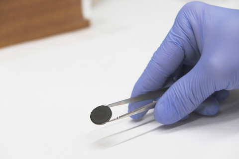
"We are going to create electroceramics using multi-material 3D printing, meaning our 3D printer can combine several materials simultaneously in a single print job," explains Bernd Wicklein, a CSIC researcher at ICMM-CSIC and the project's lead in Spain. The key to these ceramics is that they will be conductive thanks to the addition of cellulose nanoparticles (one millionth of a millimeter in size), which undergo an ultra-fast heat treatment during which they transform into conductive carbonaceous nanostructures.
To illustrate this, the researcher draws an analogy with conventional ceramics: "Anyone who works with ceramics knows that it takes many hours to turn clay into ceramic material." Now, this project will carry out that heating and calcination process in just a few minutes. "The Slovenian team uses a unique technique that reaches 1,250 degrees Celsius in just two and a half minutes," Wicklein notes. This is a highly advanced technique for manufacturing small ceramics, the kind used in the semiconductor industry.
"We want to do it so quickly because we use less electrical energy by shortening the heating process, but also the ceramic's microstructure — that is, the ordering of the particles that make up the material — becomes much more refined, finer," the scientist continues.
Biomass in the service of electronics
The project, named PRIME, will enable the one-step fabrication of electroceramic components that support semiconductor chips during their manufacturing process. This will be achieved through the combination of three mentioned elements: the addition of nanocellulose — highlighting the use of biomass for more sustainable electronics — multi-material fabrication, and an ultra-fast thermal consolidation process. "This capability allows for the direct embedding of conductive zones, heaters, electrodes, and sensors within complex ceramic parts, while maintaining the exceptional thermal, mechanical, and chemical resistance of advanced ceramics," Wicklein describes.
To demonstrate the viability of this new type of ceramic, prototypes of so-called "wafer chucks" will be produced — a kind of chip holder that combines conductive zones with heat-dissipating areas by using ceramics with different thermal properties.
"Semiconductor production relies on customized high-tech equipment that demands extreme precision, purity, and reliability," explains the scientist, noting that today these components are manufactured through multi-step processes that are "costly, energy-intensive, and limit design freedom." These limitations would be eliminated thanks to this project, which "enables the single-stage fabrication of electroceramic components that integrate conductive and insulating regions with precision within the same body, meeting strict purity and performance requirements without metallic coatings or assemblies."
Cost reduction: more sustainability, less waste
The project, led by the German start-up AMAREA Technology GmbH and involving CSIC and the Jozef Stefan Institute in Slovenia, has a synergistic action plan. First, ICMM will prepare the ceramic mixture incorporating its nanocellulose additive (based on a previous patent from the center). Then, Germany will print the components using its multi-material 3D printer, and these will be sent to Slovenia, where the heat treatment will be applied to give a ceramic structure to the printed parts. "Afterward, the material returns to Spain, where we measure that the electrical properties are as expected," Wicklein continues.
"PRIME will strengthen Europe's competitiveness in semiconductor manufacturing and high-tech equipment by establishing a new, highly efficient flexible production paradigm for functional electroceramic products," the researcher states. In fact, he assures, it will reduce manufacturing costs and energy consumption while increasing semiconductor factory performance and reducing waste rates. "We will also shorten development cycles through rapid design iteration and localized, energy-efficient European production," the scientist enumerates.
The project, which has already sparked interest in the international semiconductor industry, has more than half a dozen companies that have expressed their commitment to supporting and validating its results. Furthermore, from an environmental perspective, "PRIME demonstrates bio-based material systems and sustainable processes, substantially reducing CO2 emissions through an ultra-fast consolidation concept, efficient resource use, and reduced dependence on critical raw materials, fully aligning with the European Green Deal and circular economy principles," Wicklein concludes.
Instituto de Ciencia de Materiales de Madrid (ICMM)
Sor Juana Ines de la Cruz, 3
Cantoblanco, 28049
Madrid, España
Telephone: (+34) 91 334 90 00
Email: @email
Communication Office: @email

Acknowledge the Severo Ochoa Centres of Excellence program through Grant CEX2024-001445-S/ financiado por MICIU/AEI / 10.13039/501100011033

Contacto | Accesibilidad | Aviso legal | Política de Cookies | Protección de datos