Design and fabrication of hybrid materials with optimal symbiosis of organic semiconductors, inorganic nanoparticles and graphene properties.
Search of new or improved features of the resulting nanostructured hybrid films,
Applications: transparent electrodes and nanostructured active layers in photovoltaic cells, electroluminescent devices, field effect transistors and sensors.
Approach
Materials design and fabrication + Fundamental study of materials + Device fabrication + Technology development
Basic studies
Resonant Raman processes in graphene oxide
Chemical and thermal reduction mechanisms in few layer thin films and bulk graphene oxides.
Stacking of graphene oxide few-layer films and defects produced by thermal and chemcial rediction mechanisms
Transparent electrodes: Cheap, green, scalable to large areas, Indium free, on any substrate, in particular flexible ⇒ Graphene oxide (GO)
Optimization of chemically derived few-layer graphene films for transparent electrodes with doping control
Hybrid graphene based materials: chemically derived graphene thin films or CVD graphene with metallic, semiconductor or oxide nanoparticles.
Graphene patterning and nanostructuring - graphene quantum dots
Large scale patterning of GO and G films for integration in devices, Nano-Graphene-GQDs
Development and optimization of a novel mask-free cost-effective technique for micro/nano-patterning based on electrical micro/nano-discharges compatible with large area manufacturing.
CVD graphene and nanographene on different metal thin films.
Building a home made set-up: CVD + sputtering technique
Related Projects
“MATERIALES HIBRIDOS BASADOS EN GRAFENO PARA APLICACIONES EN ENERGIA Y DETECCION OPTICA”. Enero 2016- diciembre 2018, MAT2015-65356-C3-1.
“PHAMA 2.0, Materiales híbridos avanzados para aplicaciones fotónicas” Programa de I + D entre grupos de investigación de la Comunidad de Madrid. Proyecto concedido. 2015-2018.
“Materiales híbridos basados en grafeno para aplicaciones optoelectrónicas: optimización de sus propiedades y procesado de dispositivos de bajo coste” ICMM. MAT2012- 37276-C03-01
“Sistemas de almacenamiento de energía con grafeno para vehículos eléctricos” Proyecto Repsol-INSPIRE. UPM-CSIC. Abril 2013 – diciembre 2015
Graphene Flagship, Octobre 2013 - . Workpackage Materials
Mecanisms of the magnetoresistance, phase coexistance and segregation, inhomogeneities, distortions and local structure of magnetic oxides. Phonons and electron-phonon interactions.
Ultra thin films and heterostructures of manganese perovskites and insulating oxides. Structure, interfases, substrate effects. Effects in the magnetic and transport properties related to the nanometric scale.
Elastic constants of graphene oxide few-layer films: correlations with interlayer stacking and bonding
RJJ. Rioboo, E. Climent-Pascual, X. Diez-Betriu, F. Jimenez-Villacorta, C. Prieto, A. de Andres,
J Mater Chem C 3,4868 (2015).
Abstract
We propose a strategy to study the elastic properties of extremely thin graphene oxide (GO) films using Brillouin spectroscopy. The dependence of the surface acoustic wave of a gold capping layer on the structural, chemical and morphological changes occurring to the underneath GO film with temperature is reported and analyzed. At room temperature the shear constant c(44) is similar to 17 GPa and hardens up to 28 GPa at 100 degrees C due to the partial elimination of embedded water layers and to interlayer distance shrinking. At 200 degrees C the almost complete elimination of water induces layer stacking disorder, further GO-GO distance reduction and a significant increase of all elastic constants. The in-plane constants harden due to the partial restoration of the sp(2) C network (c(11): from 268 to 620 GPa) and the out of plane constants harden due to the H bonds that now directly connect the neighbouring GO layers (c(44) approximate to 80 GPa). The obtained Young's moduli are significantly higher than those reported for GO paper because the ultra-thin GO films are highly ordered and there is no macroscopic applied strain during the measurement. The results obtained here are associated with the intrinsic properties of GO as in-plane and inter-layer bonding.
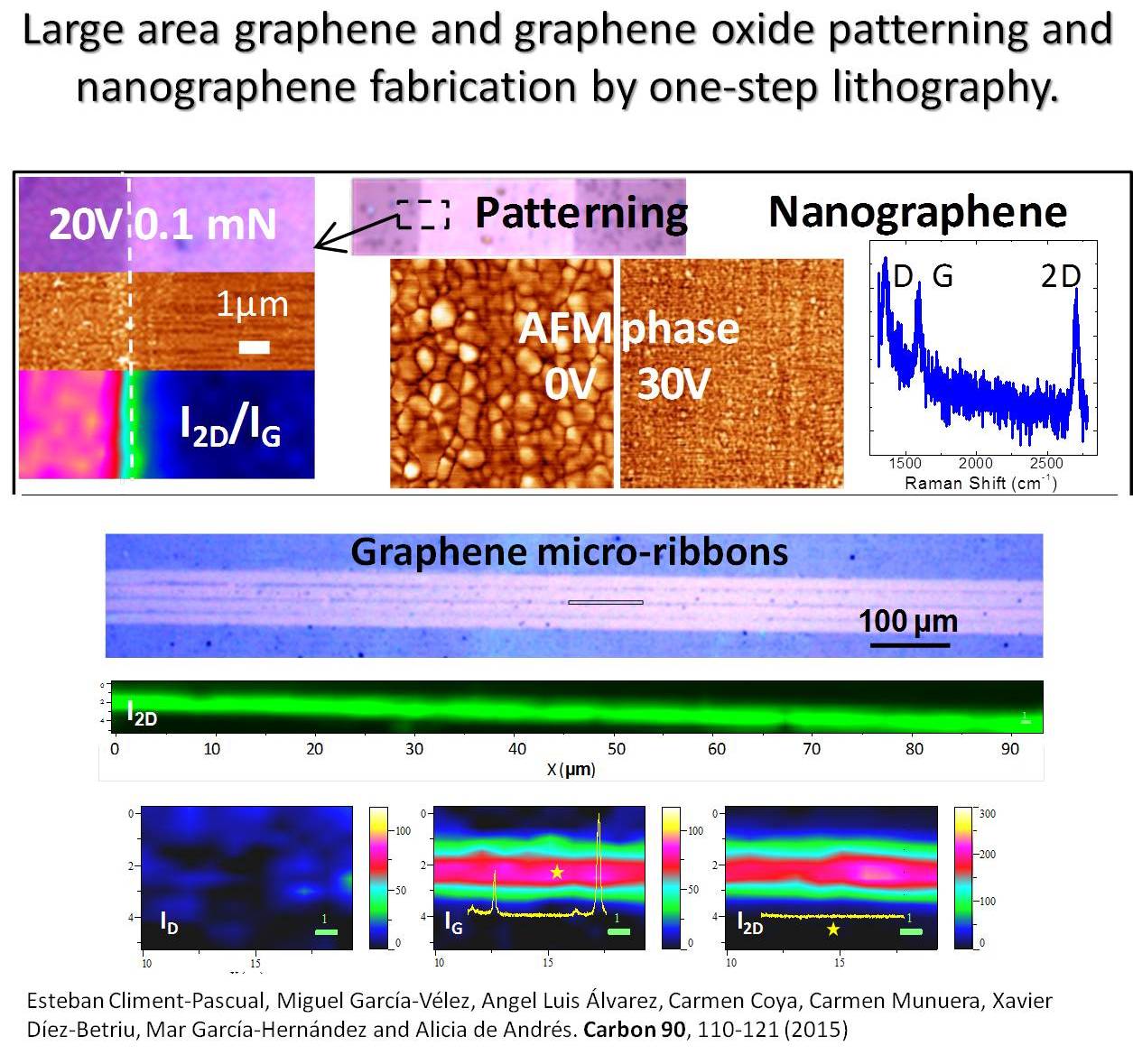
Large area graphene and graphene oxide patterning and nanographene fabrication by one-step lithography
E. Climent-Pascual, M. Garcia-Velez, AL. Alvarez, C. Coya, C. Munuera, X. Diez-Betriu, M. Garcia-Hernandez, A. de Andres,
Carbon 90,110 (2015).
Abstract
A cheap and green technology based on electro-erosion, performed at room conditions and scalable to large area (cm(2)) is demonstrated for structuring graphene and graphene oxide films on any substrate. This one-step technique based on electrical discharges produced by a direct current voltage source competes favorably with laser patterning. The threshold voltage for complete graphene elimination as determined by Raman mapping is around 20 V. At low relative humidity conditions (30%) the transformation to graphene oxide is also detected for operating voltages above 40 V, the oxidation being probably mediated by the residual adsorbed water at the surface. We also show the close correlation of atomic force microscopy (AFM) phase images with the modified graphene characteristics while AFM topographic images are dominated by extrinsic aspects. The use of a spring probe relaxes the requirement of precision for the tip-sample distance and sample flatness to around 10 inn which is very convenient for large scale applications. Furthermore, this technique allows the formation of high quality nanographene, with size around 18 nm, and graphene micro-ribbon lattices in a very fast way and very well defined edges, with dimensions down to 1 mu m width and mm length, very promising for terahertz graphene plasmonic applications. (C) 2015 Elsevier Ltd. All rights reserved.
Lactate biosensor based on a bionanocomposite composed of titanium oxide nanoparticles, photocatalytically reduced graphene, and lactate oxidase
E. Casero, C. Alonso, MD. Petit-Dominguez, L. Vazquez, AM. Parra-Alfambra, P. Merino, S. Alvarez-Garcia, A. de Andres, E. Suarez, F. Pariente, E. Lorenzo,
Microchim Acta 181,79 (2014).
Abstract
We have developed a lactate biosensor based on a bionanocomposite (BNC) composed of titanium dioxide nanoparticles (TiO2-NPs), photocatalytically reduced graphene, and lactate oxidase. Graphene oxide was photochemically reduced (without using any chemical reagents) in the presence of TiO2-NPs to give graphene nanosheets that were characterized by atomic force microscopy, Raman and X-ray photoelectron spectroscopy. The results show the nanosheets to possess few oxygen functionalities only and to be decorated with TiO2-NPs. These nanosheets typically are at least 1 mu m long and have a thickness of 4.2 nm. A BNC was obtained by mixing lactate oxidase with the nanosheets and immobilized on the surface of a glassy carbon electrode. The resulting biosensor was applied to the determination of lactate. Compared to a sensor without TiO2-NPs, the sensor exhibits higher sensitivity (6.0 mu A mM(-1)), a better detection limit (0.6 mu M), a wider linear response (2.0 mu M to 0.40 mM), and better reproducibility (3.2 %).
Graphene-oxide stacking and defects in few-layer films: Impact of thermal and chemical reduction
X. Diez-Betriu, FJ. Mompeam, C. Munuera, J. Rubio-Zuazo, R. Menendez, GR. Castro, A. de Andres,
Carbon 80,40 (2014).
Abstract
The stacking modes of graphene oxide monolayers (GO) when forming thin films is a crucial aspect determining many properties especially those related with transport. Stacking, morphology and effects of thermal and chemical reduction are studied combining in-situ synchrotron radiation diffraction and atomic force microscopy with simulations. The GO flakes mimic the substrate morphology and present an almost perfect stacking for few-layer films (2-10 layers) when in-plane flake size is large enough. The interlayer distance is found to be 1 nm irrespective of the film thickness and drastic discontinuities upon thermal annealing are observed between 100 and 200 degrees C. Moreover, the short GO-GO distance (0.38 nm) observed at temperatures (500 degrees C) where oxygen content is still high indicates that stacking is mainly governed by embedded water molecules. The large interlayer distance (0.76 nm) in chemically reduced films and its robustness against thermal annealing are due to the folding of the edges of the flakes occurring upon the elimination of the functional groups. The central part of the flakes remains extremely flat contrary to what occurs with thermal reduction. These structural defects induced by chemical and thermal reduction processes are very probably the most important limitations for electrical conductivity in GO based electrodes. (C) 2014 Elsevier Ltd. All rights reserved.
Breakdown into nanoscale of graphene oxide: Confined hot spot atomic reduction and fragmentation
G. Goncalves, M. Vila, I. Bdikin, A. de Andres, N. Emami, RAS. Ferreira, LD. Carlos, J. Gracio, PAAP Marques,
Scientific Reports 4,6735 (2014).
Abstract
Nano-graphene oxide (nano-GO) is a new class of carbon based materials being proposed for biomedical applications due to its small size, intrinsic optical properties, large specific surface area, and easy to functionalize. To fully exploit nano-GO properties, a reproducible method for its production is of utmost importance. Herein we report, the study of the sequential fracture of GO sheets onto nano-GO with controllable lateral width, by a simple, and reproducible method based on a mechanism that we describe as a confined hot spot atomic fragmentation/reduction of GO promoted by ultrasonication. The chemical and structural changes on GO structure during the breakage were monitored by XPS, FTIR, Raman and HRTEM. We found that GO sheets starts breaking from the defects region and in a second phase through the disruption of carbon bonds while still maintaining crystalline carbon domains. The breaking of GO is accompanied by its own reduction, essentially by the elimination of carboxylic and carbonyl functional groups. Photoluminescence and photothermal studies using this nano-GO are also presented highlighting the potential of this nanomaterial as a unique imaging/therapy platform.
Raman spectroscopy for the study of reduction mechanisms and optimization of conductivity in graphene oxide thin films
X. Diez-Betriu, S. Alvarez-Garcia, C. Botas, P. Alvarez, J. Sanchez-Marcos, C. Prieto, R. Menendez, A. de Andres,
J Mater Chem C 1,6905 (2013).
Abstract
Highly reduced few-layer graphene oxide films with conductivities of up to 500 S cm(-1) are obtained. The thin films with an optimized compromise between sheet resistance (3.1 k Omega sq(-1)) and transparency (around 80% to 90%) are suitable for touch screens and transparent electrodes in OLEDs. We discuss the effects of low temperature annealing and chemical reduction on the properties of the films and present an optimized reduction process that allows the original 2D/G Raman intensity ratio of few-layer graphene to be recovered. The Raman spectrum of graphene oxide is found to be only related to oxygen-free graphene-like regions with Raman bands at 1130 and 3155 cm(-1) that probably involve C-H vibrations of rings and edges, while a band at 1700 cm(-1) is assigned to irregular rings such as Stone Wales defects. All the bands involve resonant Raman processes and disappear in highly reduced samples. Clear correlations of the D band width with the sp(2) content in thin films and resistivity have been observed, indicating that this is a good Raman parameter for evaluating the quality of the samples. The structural defects produced by the release of embedded water and some of the oxygen functional groups during annealing are detrimental for intra-grain conductivity but greatly enhance inter-grain connectivity.
Comparative Response of Biosensing Platforms Based on Synthesized Graphene Oxide and Electrochemically Reduced Graphene
E. Casero, C. Alonso, L. Vazquez, MD. Petit-Dominguez, AM. Parra-Alfambra, M. de la Fuente, P. Merino, S. Alvarez-Garcia, A. de Andres, F. Pariente, E. Lorenzo,
Electroanal 25,154 (2013).
Abstract
In this work, we report the synthesis and characterization of different kinds of graphene nanomaterials and their applicability to the development of biosensing platforms. We have synthesized graphene oxide (GO) following a modified Hummers method, which has been subsequently reduced by electrochemical procedures. This reduction strategy precludes the employment of toxic solvents, leading to a product, electrochemically reduced graphene (ERG), free of contaminants. The characterization of the synthesized nanomaterials has been performed by different techniques such as X-ray diffraction spectroscopy (XRD), Raman spectroscopy, X-ray photoelectron spectroscopy (XPS), scanning electron microscopy (SEM) and atomic force microscopy (AFM). The information gathered by this combination of techniques confirms that i) the synthesis methodology affords the production of GO nanosheets, which present a typical lateral dimension of several hundreds of nanometers and a thickness value of 1.3 +/- 0.1 nm, ii) the reduction step has been successfully achieved leading to graphene nanosheets free of oxygen functionalities with an average lateral dimension of at least 1 micrometer and a thickness value of 2.8 +/- 0.2 nm. Once we have confirmed that both materials have been successfully synthesized, we have studied the effect of the effect of their inclusion in biosensing platforms on the analytical response, selecting a lactate oxidase based biosensor as a model system. We have demonstrated that although the incorporation of GO or ERG to the device results in an enhancement of the analytical response of the resulting biosensing platform, the former system offers slightly better analytical properties and a more reproducible response than the ERG one.
Carbon nanotubes-mesoporous silica composites as controllable biomaterials
M. Vila, JL. Hueso, M. Manzano, I. Izquierdo-Barba, A. de Andres, J. Sanchez-Marcos, C. Prieto, M. Vallet-Regi,
J Mater Chem 19,7745 (2009).
Abstract
A composite based on mesoporous ordered silica (SBA-15) and carbon nanotubes (CNTs), has been synthesized to be used in biomedical applications as a conductor composite for cell stimulation and regeneration. The influence of the CNT addition time on the SBA-15-CNTs composite synthesis has been studied and optimized attending to morphology and structure, to produce a homogeneous material with both structures preserved. With the addition of the CNTs, the electrical resistance has decreased 8 orders in magnitude in comparison to the SBA-15 itself. The potential of these materials to be used as bioimplants has been evaluated in vitro by soaking the composite in simulated body fluid (SBF) at 37 degrees C.
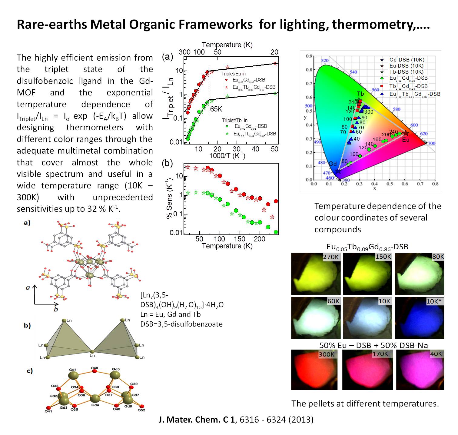
Multimetal rare earth MOFs for lighting and thermometry: tailoring color and optimal temperature range through enhanced disulfobenzoic triplet phospho
RF. D'Vries, S. Alvarez-Garcia, N. Snejko, LE. Bausa, E. Gutierrez-Puebla, A. de Andres, MA. Monge,
J Mater Chem C 1,6316 (2013).
Abstract
New isostructural compounds [Ln(7)(3,5-DSB)(4)(OH)(9)(H2O)(15)]center dot 4H(2)O (Ln = Eu, Gd and Tb) (DSB = 3,5-disulfobenzoate), with excellent optical properties, have been obtained and studied. By combining the lanthanide cations with the DSB ligand the formation of a singular heptanuclear [Ln(7)(OH)(9)](+12) metallic core secondary building unit (SBU) has been promoted. This core is defined as a bi-capped dicubane SBU, and is a 4-connected node in a bidimensional net with (4(4).6(2)) topology. The highly efficient emission from the triplet state of the disulfobenzoic ligand in the Gd-MOF and the exponential temperature dependence of I-Triplet/I-Ln = I-o exp(-E-A/k(B)T) allow the design of thermometers with different color ranges through the adequate multimetal combination that cover almost the whole visible spectrum and are useful in a wide temperature range (10-300 K) with unprecedented sensitivities up to 32% K-1. The Eu-DSB and Tb-DSB MOFs present an optimum antenna effect, a temperature independent f-f emission temporal decay and, in spite of the close packing of the Ln ions inside the MOF, no concentration quenching. The external efficiency is drastically increased in MOFs with a combination of a few percent of Eu and/or Tb with Gd by means of radiative and non-radiative energy transfers from the Gd ions and Gd connected ligands.
Optical studies of amorphous Ge nanostructures in Al2O3 produced by pulsed laser deposition
J. Martin-Sanchez, J. Toudert, R. Serna, A. de Andres, J. Garcia-Lopez,
Thin Solid Films 541,92 (2013).
Abstract
Thin films with embedded amorphous Ge nanostructures are characterised by in-situ and post-deposition techniques in order to study their size-dependent properties. The films are multilayer structures in which Ge nanostructured layers with effective thickness are separated by amorphous aluminium oxide layers (Al2O3). During deposition in-situ reflectivity measurements are used to achieve information on the amount of Ge deposited and on the Al2O3 coverage. The effective optical properties of the films were obtained from spectroscopic ellipsometry measurement analysis. Our results suggest a topological evolution of the Ge nanostructures as a function of the Ge content and the existence of size-dependent quantum confinement effects in the nanostructures. (C) 2013 Elsevier B.V. All rights reserved.
Star-shaped hexaaryltriindoles small molecules: Tuning molecular properties towards solution processed organic light emitting devices
C. Coya, C. Ruiz, AL. Alvarez, S. Alvarez-Garcia, EM. Garcia-Frutos, B. Gomez-Lor, A. de Andres,
Org Electron 13,2138 (2012).
Abstract
We present a series of differently substituted star-shaped hexaaryltriindoles with tunable light-emitting properties. The deep blue emission is unchanged by donor peripheral substituents while an increasing acceptor character produces a reduction of the optical gap, an increased Stokes shift and eventually leads to the appearance of a new electronic level and to the simultaneous deep blue (413 nm) and green (552 nm) emission in solution. Quenching by concentration increases with the acceptor character but is lower as the tendency of these compounds to aggregate is stronger. Solution processed thin films present optical and morphological qualities adequate for device fabrication and similar electronic structure compared to solutions with an emission range from 423 nm up to 657 nm (red), demonstrating the possibility of tuning the energy levels by chemical functionalization. We have fabricated and characterized single-layer solution processed organic light emitting diodes (OLED) to investigate the influence on transport and emission properties of the substituting species. We analyzed the I-V response using a single-carrier numerical model that includes injection barriers and non-uniform electric-field across the layer. As a result, we obtained the electric field dependence of the mobility for each device. Best results are obtained on the most electron rich derivative functionalized with six donor methoxy groups. This material shows the highest emission efficiency in solid state, due to aggregation-induced enhancement, and better transport properties with the highest mobility and a very low turn-on voltage of 2.8 V. The solution processed OLED devices produce stable deep blue (CIE coordinates (0.16, 0.16)) to white (CIE coordinates (0.33, 0.3)) emission with similar luminous efficiencies. (C) 2012 Elsevier B.V. All rights reserved.
Stable organic radical stacked by in situ coordination to rare earth cations in MOF materials
F. Gandara, N. Snejko, A. de Andres, JR. Fernandez, JC. Gomez-Sal, E. Gutierrez-Puebla, A. Monge,
Rsc Advances 2,949 (2012).
Abstract
With the correct choice of the solvothermal conditions, we have achieved the unprecedented in situ formation of the free radical form of the anthraquinone-1,5-disulfonate molecule, and its favorable organization. The semiquinone radicals are coordinated to rare-earth cations to produce a 2D framework with a very high charge mobility and electric conductivity through the pi-pi-interactions. The existence of AQDS(3-center dot) anion radicals is proven on the base of: i) the electrical neutrality: elemental analyses for the different lanthanide RPF-8 bulks, the maximum residual electron densities in the structure, rule out the existence of any other neutralizing ion, ii) the geometrical modifications in the antraquinone molecules, and iii) although less definitive, due to the low magnetic moment mu = 0.39 mu(B), the exhibited paramagnetism for the La (3+) with no unpaired electrons.
Synthesis and tunable emission of novel polyfluorene co-polymers with 1,8-naphthalimide pendant groups and application in a single layer-single compon
C. Coya, R. Blanco, R. Juarez, R. Gomez, R. Martinez, A. de Andres, AL. Alvarez, C. Zaldo, MM. Ramos, A. de la Pena, C. Seoane, JL. Segura,
Eur Polym J 46,1778 (2010).
Abstract
New luminescent polymers containing two individual emission species-poly(fluorene-alt-phenylene) as a blue host and variable amounts of 1,8-naphthalimide as red dopant have been designed and synthesized. Optical studies (optical absorption (OA) and steady-state photoluminescence emission (PL)) in diluted solutions and thin solid films reveal that the emission spectrum can be tuned by varying the content of 1,8-naphthalimide moieties. Although no significant interaction can be observed between both moieties in the ground state, after photoexcitation an efficient energy transfer takes place from the PFP backbone to the red chromophore, indeed, by adjusting the polymer/naphthalimide ratio it is possible to obtain single polymers which emit white light to the human eye in solid state. Energy transfer is more effective in the co-polymers than in physical mixtures of the two chromophores. We prepared single-layer electroluminescent simple devices with structure: ITO/poly(3,4-ethylenedioxythiophene)/poly(4-styrenesulfonate) (PEDOT:PSS)/ active layer/Ba/Al. With this single layer-single component device structure, white light with Commission Internationale de l'Eclairage (CIE) color coordinates (0.3, 0.42) is obtained for the electroluminescence (EL) emission with an efficiency of 22.62 Cd/A. (C) 2010 Elsevier Ltd. All rights reserved.
Crystal structure and charge-transport properties of N-trimethyltriindole: Novel p-type organic semiconductor single crystals
EM. Garcia-Frutos, E. Gutierrez-Puebla, MA. Monge, R. Ramirez, P. de Andres, A. de Andres, R. Ramirez, B. Gomez-Lor,
Org Electron 10,643 (2009).
Abstract
We report on a new p-type organic semiconductor single crystal, 5,10,15-trimethyl-10,15-dihydro-5H-diindolo[3,2-a:3',2'-c]carbazole (N-trimethyltriindole). This molecule crystallizes forming a highly ordered columnar structure in which stacked molecules are situated at two alternating distances (3.53 angstrom and 3.68 angstrom) along the column as determined by single crystal X-ray diffraction analysis. These short intermolecular distances between adjacent units, make this system an ideal candidate for charge-transport processes along the stacks. Relevant parameters for transport (i.e. internal reorganization energies, transfer integral) have been estimated by DFT calculations at a 6-311 G(d,p)/B3LYP level of theory. As a double check for the transfer integral, the electronic band structure of a one-dimensional stack of molecules has been computed. The electronic properties of this material have been studied both theoretically and experimentally. Its HOMO value is found to coincide with Au work function (Phi(Au) = 5.1 eV), thus low barriers are expected for hole injection from gold electrodes. The hole mobility of this material has been predicted theoretically considering a hopping-type mechanism for the charge-transport and determined experimentally at the space charge limited current (SCLC) regime of the current-voltage measurements. Both theoretical and experimental values are in good agreement. The high hole mobility (mu(min) = 0.4 cm(2) V(-1) s(-1)) of this material points towards its useful application in the organic electronics arena. N-Trimethyltriindole single crystals constitute an essential model to study transport properties of triindole-based materials and to design new derivatives with improved electronic performance. (C) 2009 Elsevier B.V. All rights reserved.
Full-solution-processed blue organic light emitting device based on a fluorescent 1,3,5-tristyrylbenzene stilbenoid small molecule
C. Coya, A. de Andres, C. Zaldo, AL. Alvarez, B. Arredondo, R. Gomez, JL. Segura, C. Seoane,
J Appl Phys 105,044510 (2009).
Abstract
A full-solution-processed blue organic light emitting diode display based on a small molecule built on a fluorescent stilbenoid core has been fabricated and characterized. The structure of the blue device is ITO/PEDOT:PSS/active layer/Al. The optical characterization of the 1,3,5-tristyrylbenzene endowed with alkoxy (- OC(6)H(13)) chain active layer reveals a change in the excited molecular level configuration due to the molecular packing in the thin film that gives as a result a large Stokes shift in the solid state. The electroluminescence in the deep-blue region of the single layer device corresponds well with the photoluminescence emission of the thin films (438 nm) and is independent of the applied voltage. Raman analysis confirms the stability of the compound through the fabrication process. From the I-V study, an effective hole mobility of 9.3x10(-6) cm(2)/V s for the active layer has been obtained.
A rare-earth MOF series: Fascinating structure, efficient light emitters, and promising catalysts
F. Gandara, A. de Andres, B. Gomez-Lor, E. Gutierrez-Puebla, M. Iglesias, MA. Monge, DM. Proserpio, N. Snejko,
Cryst Growth Des 8,378 (2008).
Abstract
A new family of rare-earth polymeric framework RPF-4 has been obtained and its structure solved from an intrinsically triple twinned crystal. The framework formed by a H-O bond free rare-earth matrix, with the Ln atoms separated in two directions, makes them very promising materials for light-emitting diodes. The properties of the materials as heterogeneous catalysts are reported, too. IR spectroscopy suggests the presence of a peroxo complex that acts as active species in the oxidation reaction.
Self-sterilized EVOH-TiO2 nanocomposites: Interface effects on biocidal properties
ML. Cerrada, C. Serrano, M. Sanchez-Chaves, M. Fernandez-Garcia, F. Fernandez-Martin, A. de Andres, RJJ. Rioboo, A. Kubacka, M. Ferrer, M. Fernandez-Garcia,
Adv Funct Mater 18,1949 (2008).
Abstract
Nanocomposite materials obtained by TiO2 incorporation into ethylene-vinyl alcohol copolymers, extensively used in food packaging, are prepared via a straightforward melting process. The structural characteristics of the nanocomposites are examined using wide and small angle X-ray scattering (WAXS/SAXS), and vibrational infrared and Raman spectroscopies. A microscopy (SEM/TEM) study shows that the materials obtained are highly homogeneous at the nanometric scale, exhibiting an intimate contact between both the organic and inorganic components. TiO2 incorporation into this polymer matrix renders self-sterilized nanocomposite materials upon light excitation, which are tested against nine micro-organisms (gram-positive and gram-negative bacteria, cocci, and yeasts) typically involved in food contamination and/or degradation. Overall, the nanocomposites display an impressive performance in the killing of all micro-organisms with a maximum for an oxide content between 2-5 wt %. The measurement of the physico-chemical properties together with the structural characterization of the materials provide conclusive evidence that the nanocomposites biocidal capability born of the nanometric organo-morganic interface and rationalize the existence of a maximum as a function of the TiO2 content.
Pressure induced structural transformations in catalytically active NH4[Eu(SO4)(2)] studied by light scattering
A. de Andres, J. Sanchez-Benitez, C. Cascales, N. Snejko, E. Gutierrez-Puebla, A. Monge,
Chem Phys Lett 451,106 (2008).
Abstract
Light scattering experiments have been performed under hydrostatic pressures up to 90 kbar in NH4[Eu(SO4)(2)]. This material behaves as an active catalyst and presents a layered structure with two kinds of sulfate groups bonded to Eu3(+) ions. Raman phonons related to the SO4 groups as well as Eu3(+) photoluminescence spectra evidence the induction by pressure of two discontinuous structural transformations at around 30 and 70 kbar. No signs of pressure induced disorder is detected, on the contrary, the narrower phonons correspond to the 65 kbar phase. At low pressures the structure accommodates mainly through an anisotropic compression along the a-axis perpendicular to the Eu(SO4)(2) layers. (C) 2007 Elsevier B.V. All rights reserved.
Optical study of SrAl1.7B0.3O4 : Eu, R (R = Nd, Dy) pigments with long-lasting phosphorescence for industrial uses
J. Sanchez-Benitez, A. de Andres, M. Marchal, E. Cordoncillo, MV. Regi, P. Escribano,
J Solid State Chem 171,273 (2003).
Abstract
We have studied and compared the optical properties of SrAl1.7B0.3O4:Eu, R (R = Nd, Dy) pigments that present long-lasting phosphorescence obtained by different synthesis techniques. Samples obtained by ceramic methods, in our laboratories and by an industrial process, present better phosphorescent properties than those obtained by sol-gel technique. Raman spectra show that grinding produces severe damage of the lattice. We have obtained and analyzed the Eu3+ crystal field luminescence indicating that Eu3+ is found in quite different sites comparing ceramic and sol-gel samples. Codoping, with Nd or Dy is necessary in order to reduce the Eu3+ content, in all cases. The green luminescence band, obtained under UV illumination, can be fitted to two and three components in ceramic and sol-gel samples, respectively, due to different Eu2+ sites. Eu-Dy samples present the longest and the most efficient phosphorescence. The time evolution of the afterglow is well described by a t(-1) law, up to about 2 h, indicating that the recombination process is achieved by electron-hole tunneling. (C) 2003 Elsevier Science (USA). All rights reserved.
Amorphous-nanocrystalline Al doped ZnO transparent conducting thin films
X. Diez-Betriu, R. Jimenez-Rioboo, J. Sanchez-Marcos, E. Cespedes, A. Espinosa, A. de Andres,
J Alloy Compd 536,S445 (2012).
Abstract
Al-doped ZnO films have been deposited at room temperature by means of RF sputtering under different conditions and subjected to annealing treatments looking for amorphous Transparent Conducting Oxide (TCO) films in the search for their integration into the emerging area of the flexible electronics. Structural studies have been performed as well as optical and electrical characterization. Spectroscopic ellipsometry has been used for the determination of the optical gap for films grown on Si and the films thickness. The amorphous fraction of the films (up to 86%) depends on the substrate and RF power but not on the annealing temperature up to 600 degrees C for glass substrates. The resistivity is found to be independent of the amorphous degree and correlates to the optical bandgap which presents three regimes depending on the annealing temperature. (c) 2012 Elsevier B.V. All rights reserved.
Origin of the Magnetism in Undoped and Mn-Doped SnO2 Thin Films: Sn vs Oxygen Vacancies
A. Espinosa, N. Sanchez, J. Sanchez-Marcos, A. de Andres, MC. Munoz,
J Phys Chem C 115,24054 (2011).
Abstract
SnO2 and Mn-doped SnO2 thin films have been grown by radio frequency sputtering in two different atmospheres (Ar and Ar/O-2) on Si(100) and Al2O3 (R-cut) at room temperature (RT) and at 500 degrees C. The RT films are amorphous; those grown at 500 degrees C are polycrystalline or epitaxial, depending on the substrate. All the films, undoped or Mn-doped, present a paramagnetic signal, and ferromagnetism is not observed, regardless of the growth conditions or their structure. The measured magnetization systematically decreases when the films are grown in oxygen-free atmosphere, thus indicating that magnetism is not promoted by oxygen vacancies, and no correlation is found between conductivity and magnetism. We compare the experimental results with ab initio density functional calculations and demonstrate that the Sn vacancies are the origin of the measured magnetization in SnO2 undoped films. Oxygen vacancies contribute to neither the magnetic moment nor the conductivity of the samples. The localized nature of the defect-induced electronic levels prevents a collective magnetic or conducting behavior.
Confinement effects on the low temperature magnetic structure of MnP nanocrystals
A. de Andres, R. Ramirez-Jimenez, M. Garcia-Hernandez, S. Lambert-Milot, RA. Masut,
Appl Phys Lett 99,182506 (2011).
Abstract
The low temperature magnetic properties of MnP nanocrystals (15-40 nm), both in GaP:MnP epilayers and MnP films, are significantly different compared to bulk and cannot apparently be explained by differences in the structure. A simple model of localized spins is used to describe the magnetic screw structure confined to nanocrystals. The results indicate that the observed magnetic behaviour is related to the nanometric size and to changes in the coupling constants most probably localized at an external grain shell. The nucleation of helical regions at the surface of the ferromagnetic grains is proposed as a possible mechanism for the reversal of the magnetization. (C) 2011 American Institute of Physics. [doi: 10.1063/1.3658393]
MnP films and MnP nanocrystals embedded in GaP epilayers grown on GaP(001): Magnetic properties and local bonding structure
A. de Andres, A. Espinosa, C. Prieto, M. Garcia-Hernandez, R. Ramirez-Jimenez, S. Lambert-Milot, RA. Masut,
J Appl Phys 109,113910 (2011).
Abstract
MnP nanostructures embedded in GaP epilayers, and MnP polycrystalline films, grown from the vapor phase on GaP(001) substrates using metalorganic precursors are compared with bulk MnP. We observe a large increase of the low transition temperature from the ferromagnetic to the antiferromagnetic screw phase, from T(N) = 47 K for bulk to 82 K for nanocrystals in MnP:GaP films, while the Curie temperature T(C), close to room temperature, varies only slightly. A net magnetic moment is measured in the nanocrystals and films at 5 K, as well as large coercive fields, contrary to bulk MnP. X-ray absorption spectroscopy and diffraction show that epilayers and films contain MnP grains in the nanometric range with average Mn-P bond lengths very close to those of bulk MnP. The MnP film lattice parameters are almost identical to bulk values (within 0.5%) and the main crystallographic preferential orientations are those also present in the epilayers but with different relative populations. Overall the local structures of all MnP forms are very similar, except for indications of more disorder in the nanocrystals. Such combined changes of T(N) and T(C) are in apparent contradiction with the known response of bulk MnP to strains induced by hydrostatic, uniaxial or chemical pressure. We conclude that the differences in the low temperature magnetic behavior are most probably originated by local structural disorder at the surface of the nanostructures and by finite size effects. (C) 2011 American Institute of Physics. [doi:10.1063/1.3580270]
Ferromagnetism in SnO2-based multilayers: Clustering of defects induced by doping
A. Espinosa, M. Garcia-Hernandez, N. Menendez, C. Prieto, A. de Andres,
Phys Rev B 81,064419 (2010).
Abstract
Several series of A/SnO2 and Mn/B multilayers, where A and B are thin layers (0.4-10.1 nm) of SnO2, SiO2, Si, Al, Mn, or MnOx, have been investigated magnetic, electronic, and structurally. The study demonstrates that the detected ferromagnetism is related to regions of high density of defects in SnO2 induced by doping under particular conditions. The observed room-temperature ferromagnetic (RTFM) signal does not scale to Mn content but increases with the number of interfaces and their roughness. The presence of Mn in 3+ oxidation state in the SnO2 lattice is a necessary condition but is not enough to promote ferromagnetism which also requires the presence of Sn2+. The high oxygen deficiency induced by Mn doping in the tin-oxide layers is mostly compensated by the formation of the stable SnO phase. Moreover, the RTFM signal decreases upon annealing either in O-2 rich or in vacuum atmospheres. The combination of Mn with SiO2, Si, or Al produces paramagnetic signals but no ferromagnetism; consequently SnO2 is a crucial ingredient of this RTFM. The observed ferromagnetism may be explained by short-range ferromagnetic correlations between Mn probably mediated by induced holes at oxygen sites of SnO2 in the vicinity of trivalent Mn3+ doping ions. The inhomogeneous Mn distribution inside tin oxide at the multilayer interfaces may produce large enough regions with high defect concentration to allow long-range ferromagnetic order. All undoped SnO2 films, grown in a wide set of different conditions, show paramagnetic signals with high-J values but no ferromagnetism is detected probably because of the high density of defects required to establish a ferromagnetic order based in a short-range mechanism.
Induced ferromagnetism in Mn3N2 phase embedded in Mn/Si3N4 multilayers
E. Cespedes, E. Roman, Y. Huttel, J. Chaboy, J. Garcia-Lopez, A. de Andres, C. Prieto,
J Appl Phys 106,043912 (2009).
Abstract
Room temperature ferromagnetism has been obtained for different sets of Mn/Si3N4 multilayers prepared by sputtering. In order to find the most suitable conditions to stabilize the ferromagnetic ordering in this system, the evolution of the magnetic properties has been studied for films in which the Si3N4 layer thickness was maintained constant while that of the Mn layer was varied, [Mn(t(m))/Si3N4(3.4 nm)](n), and conversely, in [Mn(0.7 nm)/Si3N4(t(sn))](43) samples, in which the Mn layer thickness was kept constant while varying the Si3N4 layer thickness. Structural, compositional, electronic and magnetic characterizations have been performed by means of x-ray reflectometry, Rutherford backscattering spectrometry, x-ray photoemission spectroscopy, x-ray absorption, and superconducting quantum interference device for further knowledge of the magnetic-structural relationship in this system. Our results show that the peculiar magnetic behavior of these films is mainly related to the stabilization of a slightly distorted Mn3N2 phase that is induced by the Si3N4 at the interfaces. For samples with larger Mn layer thickness, metallic Mn and Mn3N2 phases coexist, which leads to a reduction of the total magnetization per Mn atom due to the presence of metallic Mn. For small Mn layer thickness (t(m) <0.86 nm), where noncontinuous Mn3N2 layers are formed, the magnetization decreases noticeably due to the superparamagnetic size limit. It has been found that the best conditions for the stabilization of the ferromagnetism in this system occur when both, the manganese-rich and the silicon nitride layers, are continuous and with similar thickness, close to 3.5 nm. (C) 2009 American Institute of Physics. [DOI: 10.1063/1.3203997]
X-ray absorption and magnetic circular dichroism characterization of a novel ferromagnetic MnNx phase in Mn/Si3N4 multilayers
E. Cespedes, Y. Huttel, L. Martinez, A. de Andres, J. Chaboy, M. Vila, ND. Telling, G. van der Laan, C. Prieto,
Appl Phys Lett 93,252506 (2008).
Abstract
Ferromagnetism above room temperature has been observed in Mn/Si3N4 multilayered films for the first time. Characterization of the structural and electronic properties was performed to study the ferromagnetic behavior of this system. X-ray absorption spectroscopy at the Mn K and L edges, as well as x-ray magnetic circular dichroism, evidences the presence of divalent Mn in the films. X-ray absorption near edge structure measurements, which are compared to calculations, confirms the presence of a slightly distorted Mn3N2 phase that is proposed to be the origin of the ferromagnetism in this system.
Structural study of undoped and (Mn, In)-doped SnO2 thin films grown by RF sputtering
A. Espinosa, N. Menendez, C. Prieto, A. de Andres,
J Non-cryst Solids 354,5269 (2008).
Abstract
Undoped and 5%(Mn, In)-doped SnO2 thin films were deposited on Si(1 0 0) and Al2O3 (R-cut) by RF magnetron sputtering at different deposition power, sputtering gas mixture and substrate temperature. X-ray reflectivity, was used to determine the films thickness (10-130 nm) and roughness (similar to 1 nm). The combination of X-ray diffraction and Mossbauer techniques evidenced the presence of Sn4+ in an amorphous environment, for as-grown films obtained at low power and temperature, and the formation of crystalline SnO2 for annealed films. As the deposition power, substrate temperature or O-2 proportion are increased, SnO2 nanocrystals are formed. Epitaxial SnO2 films are obtained on Al2O3 at 550 degrees C. The amorphous films are quite uniform but a more columnar growth is detected for increasing deposition power. No secondary phases or segregation of dopants were detected. (c) 2008 Elsevier B.V. All rights reserved.
Metal-organic vapor phase epitaxy of crystallographically oriented MnP magnetic nanoclusters embedded in GaP(001)
S. Lambert-Milot, C. Lacroix, D. Menard, RA. Masut, P. Desjardins, M. Garcia-Hernandez, A. de Andres,
J Appl Phys 104,083501 (2008).
Abstract
Hybrid ferromagnetic-semiconductor GaP: MnP thin films were grown at 650 S C by metal-organic vapor phase epitaxy on GaP(001) using trimethylgallium, tertiarybutylphosphine, and methyl cyclopentadienyl manganese tricarbonyl (MCTMn). Overall Mn concentrations in the hybrid films, determined by Rutherford backscattering spectrometry, were found to be nearly proportional to the MCTMn precursor gas flow rate and ranged from 2 to 3.5 at. %. Cross-sectional transmission electron microscopy (TEM) analyses revealed the presence of a homogeneous distribution of 15-30 nm wide nanoclusters in a dislocation-free GaP matrix that is fully coherent with the substrate. The nanocluster facets are predominantly aligned along the (220) planes of the GaP matrix and selected-area electron diffraction patterns in TEM indicate that the nanoclusters are coherent (or semicoherent) with the single-crystal GaP matrix. The Mn: P composition ratio in the nanoclusters was determined to be 1.00 +/- 0.05 from parallel electron energy loss spectroscopy analyses. Increasing the MCTMn flow rate during film growth resulted in an increased concentration of MnP nanoclusters in the epilayer while their dimensions remained virtually unchanged. Magnetometric characterization indicates a ferromagnetic order, with a Curie temperature of about 294 K, originating from the MnP clusters. (C) 2008 American Institute of Physics. [DOI: 10.1063/1.2992558]
High temperature ferromagnetism in mn based multilayers of wide gap semiconductors: Mn/ZnO and Mn/SnO2: the role of interfaces
A. Espinosa, E. Cespedes, C. Prieto, M. Garcia-Hernandez, A. de Andres,
J Korean Phys Soc 52,1394 (2008).
Abstract
We have investigated magnetic, electronic and structural properties of two series of multilayers, (Mn-(d)/ZnO(3 nm))(N) and (Mn-(d)/SnO2(3 nm))(N), deposited onto Si(100) using magnetron sputtering. The nominal Mn layer thickness, d, ranged from 10 to 0.2 nm and the number of layers, N, was increased to keep the total amount of Mn constant. Structural information was deduced from Xray reflectivity and XAS and Mn oxidation state is estimated from its K edge. The ferromagnetic transition temperature, T-C, in those samples where a ferromagnetic order is established, is always above 400 K. The ferromagnetic fraction within each sample evidences an opposite behaviour as Mn layer thickness is reduced and N increased, in ZnO and SnO2 series. While ferromagnetism is favoured in Mn/ZnO increasing d, the maximum value, in Mn/SnO2, is obtained for 0.4 nm Mn layers. A Mn mixed valence state is not a sufficient condition for ferromagnetism. We discuss the origin of this opposite behaviour which is related to the particular phases formed at the interfaces related to the different ability of ZnO and SnO2 to participate and saturate Mn oxide phases.
Interface and Mn valence effects in ferromagnetic insulating multilayers based on Mn and tin oxide
A. Espinosa, E. Cespedes, C. Prieto, M. Garcia-Hernandez, J. Rubio-Zuazo, A. de Andres,
J Appl Phys 103,07D129 (2008).
Abstract
Several series of Mn based multilayers (Mn/SnO(2),Mn/Si, and Mn/SiO(2))(N) were prepared by magnetron sputtering on Si(100) substrates at room temperature (RT). A ferromagnetic phase with T(C) above 300 K is detected only for Mn/SnO(2). The highest ferromagnetic signal corresponds to the presence of Mn in a mixed valence state combined with the presence of tin oxide. Grazing incidence high-angle x-ray diffraction revealed the formation of MnO and SnO(1+x) nanocrystals. After annealing, no traces of metallic Mn or MnO are detected from x-ray absorption near-edge structure (XANES) or diffraction; Mn(2)O(3) and Mn(3)O(4) oxides and polycrystalline SnO(2) were identified. A clear ferromagnetic signal below 42 K with high coercive field is then detected corresponding to Mn(3)O(4) but the RT ferromagnetic component decreases drastically. No mixed Mn-Sn-O phases are detected in as-grown or annealed samples. The close vicinity of MnO(1+x) and SnO(1+x) nanograins at the multilayer interfaces seems to be the condition necessary for the RT ferromagnetism. (c) 2008 American Institute of Physics.
Magnetic and optical characterization of ferromagnetic SnO2/Mn multilayers
A. Espinosa, C. Prieto, M. Garcia-Hernandez, A. de Andres,
J Magn Magn Mater 316,E207 (2007).
Abstract
We have investigated the magnetic and structural properties of Mn/SnO2 multilayers deposited onto Si(1 0 0) substrates at room temperature using the magnetron sputtering method. The nominal Mn layer thickness ranged from 0.4 up to 10 nm. The multilayers structure was studied by X-ray and optical reflectivity. Magnetic measurements indicate the presence of two distinct contributions. One is ferromagnetic with an order temperature above 400 K for all samples and another paramagnetic. Both ferromagnetic and paramagnetic susceptibilities per Mn atom increase as the Mn layer thickness in the multilayers is reduced, corresponding to a more diluted situation. Oscillations in the optical reflectivity measurements are only observed for the sample with nominal Mn layer thickness of 0.4 nm (75 bilayers). In this case, the disappearance of the continuous Mn layers and therefore of the interfaces preserve the necessary transparency. In multilayers with thicker Mn layer, the effective absorption coefficient increases. (c) 2007 Elsevier B.V. All rights reserved.
Correlation between Mn oxidation state and magnetic behavior in Mn/ZnO multilayers prepared by sputtering
E. Cespedes, J. Garcia-Lopez, M. Garcia-Hernandez, A. De Andres, C. Prieto,
J Appl Phys 102,033907 (2007).
Abstract
Compositional, microstructural, and magnetic characterization of [ZnO(30 A)/Mn(x)](n) multilayers prepared by sputtering is presented to study the observed ferromagnetism in the Mn-ZnO system. The nominal Mn layer thickness, x, is varied from 3 to 60 angstrom, while the: number of bilayers, n, is increased to maintain the total amount of Mn constant. Microstructure information was deduced from x-ray reflectivity, Mn oxidation state was determined by x-ray absorption spectroscopy, and magnetic properties were measured over a temperature range of 5-400 K. Magnetic behavior of these samples is found to be related to the Mn layer thickness (x). Multilayers with x >= 30 angstrom exhibit ferromagnetism with a Curie temperature above 400 K, while mostly paramagnetic behavior is obtained for x < 15 angstrom. Magnetic behavior is discussed in terms of electronic and structural parameters of samples. Mn-ZnO interface effect is related to the ferromagnetic order of the samples, but it is not a sufficient condition. The essential role of the Mn oxidation state in the magnetic behavior of this system is pointed out. It is shown a correlation between the obtained ferromagnetism and a Mn oxidation state close to 2+. (c) 2007 American Institute of Physics.
Ferroelectric substrate effects on the magnetism, magnetotransport, and electroresistance of La0.7Ca0.3MnO3 thin films on BaTiO3
A. Alberca, C. Munuera, J. Tornos, FJ. Mompean, N. Biskup, A. Ruiz, NM. Nemes, A. de Andres, C. Leon, J. Santamaria, M. Garcia-Hernandez,
Phys Rev B 86,144416 (2012).
Abstract
La0.7Ca0.3MnO3 optimally doped epitaxial films were grown on ferroelectric BaTiO3 substrates. Electronic transport (magnetoresistance and electroresistance) and magnetic properties showed important anomalies in the temperature interval between 60 and 150 K, below the metal-insulator transition. Scanning probe microscopy revealed changes in BaTiO3 surface morphology at those temperatures. La0.7Ca0.3MnO3 thickness is a critical factor: 120-angstrom -thick films showed large anomalies sensitive to electric poling of the BaTiO3, whereas the behavior of 150-angstrom -thick films is closer to that of the reference La0.7Ca0.3MnO3 samples grown on SrTiO3. We propose that, through inhomogenous strain and electric polarization effects, the ferroelectric substrate induces an inhomogenous spin distribution in the magnetic layer. This would imply the coexistence of in-plane and out-of-plane ferromagnetic patches in La0.7Ca0.3MnO3, possibly interspersed with antiferromagnetic regions, as it has recently been theoretically predicted. Substrate poling effects are investigated, and a magnetoelectric coupling is demonstrated.
Exotic magnetic anisotropy map in epitaxial La0.7Ca0.3MnO3 films on BaTiO3
A. Alberca, NM. Nemes, FJ. Mompean, N. Biskup, A. de Andres, C. Munuera, J. Tornos, C. Leon, A. Hernando, P. Ferrer, GR. Castro, J. Santamaria, M. Garcia-Hernandez,
Phys Rev B 84,134402 (2011).
Abstract
We report the observation between 40 and 120 K of anomalous magnetic hysteresis loops in thin epitaxial films of La0.7Ca0.3MnO3 grown on ferroelectric BaTiO3. These hysteresis loops display extremely unusual features: after switching at coercivity, the magnetization overshoots the eventual high-field value. We study the strains in the film and substrate with x-ray diffraction and propose a model of two magnetic moment populations with different magnetoelastic anisotropies. The relative weights of both populations can be estimated by comparison with twin samples of La0.7Ca0.3MnO3 films on nonferroelectric SrTiO3. We propose that the observed magnetization overshoots the result from differences in the magnetostriction balance as the applied magnetic field increases. The picture of a nonuniform strain field in La0.7Ca0.3MnO3 on BaTiO3, caused by the corrugation of the ferroelectric domains in the rhombohedric phase of BaTiO3, is compatible with the magnetic granular behavior observed in the temperature and field dependences of the magnetization as well as in the low temperature magnetoresistance exhibited by the epitaxial film.
Enhancement of the Curie Temperature along the Perovskite Series RCu(3)Mr(4)O(12) Driven by Chemical Pressure of R3+ Cations (R = Rare Earths)
J. Sanchez-Benitez, JA. Alonso, MJ. Martinez-Lope, A. de Andres, MT. Fernandez-Diaz,
Inorg Chem 49,5679 (2010).
Abstract
The compounds of the title series have been prepared from citrate precursors under moderate pressure conditions (P = 2 GPa) and 1000 degrees C in the presence of KCIO4 as oxidizing agent. The crystal structures are cubic, space group Im (3) over bar (No. 204); the unit cell parameters linearly vary from a = 7.3272(4) angstrom (R = La) to a = 7.2409(1) angstrom (R = Lu) at room temperature. A neutron or synchrotron X-ray diffraction study of all the members of the series reveals an interesting correlation between some structural parameters and the magnetic properties. The electron injection effect upon replacement of Ca2+ with R3+ cations in the parent CaCu3Mn4O12 oxide leads to a substantial increment of the ferrimagnetic Curie temperature (T-C). An essential ingredient is supplied by the internal pressure of the R3+ cations upon a decrease in size along the rare-earth series, from La to Lu: the concomitant compression of the MnO6 octahedral units for the small rare earths provides progressively shorter Mn-O distances and improves the overlapping between Mn and O orbitals, thereby promoting superexchange and enhancing T-C by 50 K along the series. This interaction is also reinforced by a ferromagnetic component that depends on the local distortion of the MnO6 octahedra, which also increases along the series, constituting an additional factor, via intersite virtual charge transfer t-e orbital hybridization, for the observed increment of T-C.
Anisotropy, orbital order, and colossal electroresistance in untwinned La0.9Sr0.1MnO3 single crystals
A. de Andres, N. Biskup, M. Garcia-Hernandez, YM. Mukovskii,
Phys Rev B 79,014437 (2009).
Abstract
A magnetic and electric transport study of twinned and untwinned La1-xSrxMnO3 single crystals, with Sr content corresponding to a vertical phase diagram boundary (x approximate to 0.1), is presented. The phases distinctive of both phase diagram sides are consecutively detected. All magnetic, transport, and electroresistance properties are found to be anisotropic. Below the ferromagnetic ordering, T-C1=143 K, we have detected a second magnetic transition (T-C2=125 K) with an easy ferromagnetic direction along the c axis and antiferromagnetic order (AF) along the a and/or b axes. The glassylike behavior of the ferromagnetic phase disappears when the AF correlations become long ranged. The magnetocrystalline anisotropy remains below the orbital ordering transition (T-C3=73 K) with a strong anomaly in the coercive field at 30 K. The system is insulating at any temperature with different activation energies depending on the direction of the current below T-C1. The observed magnetic anisotropy below T-C2 is consistent with a homogeneous picture of the system as the ordered orbital polaron lattice proposed for the x=0.125 compound. Typical negative magnetoresistance (MR) for single crystals is detected, except at temperatures between both magnetic transitions, T-C3 < T < T-C2, where the positive MR is due to the promotion of the orbital order. Applied magnetic fields up to 14 T could not remove the orbital order while low-current densities (j=10(-8) A/cm(2) at T=20 K), when applied along the AF axes, are able to destroy the orbital order and delocalize the carriers inducing a metalliclike conductivity and reducing the resistivity by a factor of up to 10(7). The observation of anisotropic electroresistance (ER) both in continuous and pulsed regimes, consistent with magnetic and transport anisotropies, as well as the low-current densities necessary to induce the phase transition, excludes Joule heating as the origin of the discontinuous high to low resistance transitions in these single crystals.
Persistent ferromagnetism in antiferromagnetic Pr0.6Ca0.4MnO3
N. Biskup, A. de Andres, M. Garcia-Hernandez,
Phys Rev B 78,184435 (2008).
Abstract
We report on the magnetic-field-driven persistent ferromagnetic (FM) state in antiferromagnetic (AF) manganite Pr1-xCaxMnO3, where x=0.4 and 0.375. At low temperatures the magnetic field-induced ferromagnetism (FIFM) persists even at B=0 and is quenched to a fractional value of the total number of spins. This incomplete ferromagnetism decreases with increasing temperature and disappears at T-m=10-20 K. T-m depends on the hole concentration "x" and increases as x-->0.3. We interpret this as the incomplete relaxation from FM toward AF spin orientation, resulting in the canted antiferromagnetism (CAF). This is in contrast to the "virgin" (zero-field cooled) magnetic ground state where no ferromagnetic component could be detected. Due to the strong competition between FM and AF orders, three successive AF transitions are detected. The low-temperature transition at T-3= 27 K has a strong influence on FIFM, resulting in the minimum magnetic field required to trigger the FIFM state. Furthermore, the T-3=27 K transition results in a pronounced anomaly in the temperature variation in magnetization. We comment on this property in the light of a similar finding in the phase-separated La0.21Pr0.42Ca3/8MnO3 which was interpreted as the strain-glass transition.
Colossal electroresistance without colossal magnetoresistance in La0.9Sr0.1MnO3
N. Biskup, A. de Andres, NM. Nemes, M. Garcia-Hernandez, KV. Glazyrin, YM. Mukovskii,
Appl Phys Lett 90,222502 (2007).
Abstract
The authors report on colossal electroresistance (ER) in the ferromagnetic insulator manganite La0.9Sr0.1MnO3. The single crystal samples exhibit a transition into a low resistive state above a certain threshold current. Pulsed measurements demonstrate that this transition is not a consequence of heating. ER behaves similarly to magnetoresistance (MR) above the orbital order temperature T-OO. Below T-OO the MR is only 20% while ER enhances the conductivity by several orders of magnitude. Magnetic field and electric current have opposite effects on the conductivity, therefore, it seems that only the injected carriers are able to modify the ordering of e(g) Mn orbitals. (C) 2007 American Institute of Physics.
Electroelasticity in charge ordered Pr5/8Ca3/8MnO3
N. Biskup, A. de Andres,
Phys Rev B 74,184403 (2006).
Abstract
We report on nonlinear current-voltage characteristics in single-crystal Pr5/8Ca3/8MnO3 and polycrystalline Pr0.6Ca0.4MnO3. Measurements are done with samples immersed in liquid nitrogen, aiming to reduce the effect of Joule heating. Negative differential resistance (NDR) is observed for currents as low as 1 mA. Superimposed to NDR, we observe discontinuous transitions to higher or lower resistive states. These transitions are observed and studied with current passing along all three perpendicular axes of single crystal showing clear anisotropy. In polycrystal, these transitions appear to be a mixture of transitions in different current directions of the single crystal. We demonstrate that the above effects are not originated by Joule heating, and we discuss their possible origin.
Nonlinear electrical characteristics of the low-bandwidth manganites R1-xCaxMnO3(R=Pr,Nd,Ho,Er; x=0.3-0.5)
N. Biskup, A. de Andres, IM. Ochando, MT. Casais,
Phys Rev B 73,184404 (2006).
Abstract
We have investigated nonlinear electrical characteristics in low bandwidth manganites R1-xCaxMnO3 with R=Pr,Nd,Ho,Er and x=0.3-0.5. In all these materials we observe strong nonlinear I-V characteristic that is manifested in negative differential resistance (NDR) and breakdown voltages V-br as low as few volts. These effects are accompanied by intense Joule heating that seems to be inseparable from the effect itself. We present different types of measurements with the aim to resolve the origin of the phenomena. Melting of insulating state is observed regardless of its origin-antiferromagnetic, charge ordered, or paramagnetic. This nonlinearity is found to have microscopic origin, indicating that it is some sort of percolation effect. Hysteretic effects also indicate that the heating is not the only cause of NDR. Enhancement of conductivity is proposed to arise from double exchange induced by local magnetic field.
Suppression of ferromagnetic double exchange by vibronic phase segregation
F. Rivadulla, M. Otero-Leal, A. Espinosa, A. de Andres, C. Ramos, J. Rivas, JB. Goodenough,
Phys Rev Lett 96,016402 (2006).
Abstract
From Raman spectroscopy, magnetization, and thermal expansion on the system La-2/3(Ca1-xSrx)(1/3)MnO3, we have been able to provide a quantitative basis for the heterogeneous electronic model for manganites exhibiting colossal magnetoresistance (CMR). We construct a mean-field model that accounts quantitatively for the measured deviation of T-C(x) from the T-C predicted by de Gennes double-exchange in the adiabatic approximation and predicts the occurrence of a first-order transition for a strong coupling regime, in accordance with the experiments. The existence of a temperature interval T-C< T < T-*, where CMR may be found, is discussed in connection with the occurrence of an idealized Griffiths phase.
Peculiar magnetic behavior of the TbCu3Mn4O12 complex perovskite
J. Sanchez-Benitez, JA. Alonso, A. de Andres, MJ. Martinez-Lope, JL. Martinez, A. Munoz,
Chem Mater 17,5070 (2005).
Abstract
TbCU3Mn4O12 perovskite has been prepared in polycrystalline form under moderate pressure conditions of 2 GPa, in the presence of KClO4 as oxidizing agent. This material has been studied by X-ray and neutron powder diffraction (XRD and NPD) and magnetotransport measurements. The crystal structure is cubic, space group Im (3) over bar (No. 204), with a = 7.2668(1) angstrom at room temperature (RT). This compound presents a ABO(3) perovskite superstructure, where the A positions are occupied by Tb and Cu, ordered in a 1:3 arrangement, giving rise to the body centering of the unit cell. At the B positions, Mn adopts a mixed oxidation state of 3.75+: MnO6 octahedra are considerably tilted by 19 degrees, due to the relatively small size of the A-type cations. TbCu3Mn4O12 is ferrimagnetic below T-C = 395 K: the magnetic structure, studied by NPD, reveals that Mn and Cu spins are ordered below T-C in an antiparallel arrangement. Additionally, below 100 K the Tb magnetic moments also participate in the magnetic structure, becoming antiferromagnetically coupled to Mn spins. This arrangement can be broken under the presence of an external magnetic field, inducing a turnover of the Tb magnetic moments, which then become parallel to the Mn moments. The mixed valence state created at the Mn sublattice is responsible for the observed metallic behavior; a negative magnetoresistance of 25% is achieved at 5 K for H = 9 T.
Huge magnetoresistance in ultrathin La0.7Ca0.3MnO3 films: The role of superparamagnetic clusters and domain walls
JM. Colino, A. de Andres,
Appl Phys Lett 87,142509 (2005).
Abstract
The magnetic behavior of epitaxial La0.7Ca0.3MnO3 (LCMO) films grown on SrTiO3, with thickness down to 2.4 nm, has been analyzed and correlated to the magnetoresistance (MR). Below about 10 nm the canonical ferromagnetic order switches to a distribution of superparamagnetic clusters. These ultrathin films show a huge MR (4000%) at T-c and, at 5 K, the MR is 300 times that of the ferromagnetic films' value. Metallic conductivity is observed below T-c down to the blocking temperature (T(B)approximate to 65 K) but a strong upturn appears below T-B. These findings can be explained by the ordering of uncoupled superparamagnetic clusters and their blocking at lower temperature, together with the collapse of the magnetic domain walls which are substituted by very small Mn magnetic clusters (few Mn) probably localized at the structural domain boundaries. (C) 2005 American Institute of Physics.
Origin of the colossal dielectric response of Pr0.6Ca0.4MnO3
N. Biskup, A. de Andres, JL. Martinez, C. Perca,
Phys Rev B 72,024115 (2005).
Abstract
We report the detailed study of dielectric response of Pr0.6Ca0.4MnO3 (PCMO), a member of the manganite family showing colossal magnetoresistance. Measurements have been performed on four polycrystalline samples and four single crystals, allowing us to compare and extract the essence of dielectric response in the material. High-frequency dielectric function is found to be epsilon(HF)=30, as expected for the perovskite material. Dielectric relaxation is found in the frequency window of 20 Hz to 1 MHz at temperatures of 50-200 K that yields to colossal low-frequency dielectric function, i.e., the static dielectric constant. The static dielectric constant is always colossal, but varies considerably in different samples from epsilon(0)=10(3) to 10(5). The measured data can be simulated very well by blocking (surface barrier) capacitance in series with sample resistance. This indicates that the large dielectric constant in PCMO arises from the Schottky barriers at electrical contacts. Measurements in magnetic field and with dc bias support this interpretation. Colossal magnetocapacitance observed in the title compound is thus attributed to extrinsic effects. Weak anomaly at the charge ordering temperature can also be attributed to interplay of sample and contact resistance. We comment on our results in the framework of related studies by other groups.
Evidence of two different Mn states in CaCu3Mn4O12 derivatives with colossal magnetoresistance
J. Sanchez-Benitez, C. Prieto, A. de Andres, JA. Alonso, MJ. Martinez-Lope, MT. Casais,
Phys Rev B 70,024419 (2004).
Abstract
A new series of magnetoresistive oxides based on the CaCu3Mn4O12 perovskite has been investigated by x-ray absorption and neutron powder diffraction. The samples were either doped at Cu sites by Mn or by La at Ca sites. The x-ray absorption near edge spectroscopy spectra evidence the presence of two different Mn K-edges corresponding to the two notably different crystallographic environments where Mn locates. Mn3+, with localized e(g) electrons is distributed at random with Cu2+ cations at the strongly distorted A positions of the perovskite, while valence mixing Mn3+/Mn4+ occurs at the standard B site of the perovskite. The metallic behavior of the conductivity is due to the partial filling of the e(g) band of the Mn ions located at the B sublattice. The different behaviors of the two edges evidence the role of the structure on the electronic levels of the absorbing ion. Valence mixing occurs at the regular Mn(B) site of the perovskite, where no signatures of individual Mn3+ and Mn4+ edges are detected, and conversely, the energy levels of Mn ions at different crystallographic sites are decoupled.
Doping effects on the valence band of Tl2Mn2O7 pyrochlores: Relation to magnetoresistance
J. Sanchez-Benitez, A. de Andres, C. Prieto, J. Avila, L. Martin-Carron, JL. Martinez, JA. Alonso, MJ. Martinez-Lope, MT. Casais,
Appl Phys Lett 84,4209 (2004).
Abstract
Photoemission and x-ray absorption near edge spectroscopy measurements have been performed in Tl2Mn2O7 oxides doped with 10% different ions, Bi, Cd, or Sb, which produce colossal changes in the magnetoresistance values. The contributions to the valence band related to Mn, O, and the doping ions have been obtained. We found that the paramagnetic phase of doped Tl pyrochlores is charge-transfer insulator type with oxygen character of the upper edge of the valence band. Bi 6s and Cd 4d orbitals lie also at the upper edge of the valence band. Mn valence is identical for all samples while oxygen content varies to compensate for the charge introduced by doping. The density of carriers, which is correlated to the magnetoresistance values, is determined by the density of states near the Fermi level provided by Tl and O content. (C) 2004 American Institute of Physics.
Excitations of the orbital order in RMnO3 manganites: Light scattering experiments
L. Martin-Carron, A. de Andres,
Phys Rev Lett 92,175501 (2004).
Abstract
Raman spectroscopy was used to seek out the orbital excitations in orbitally ordered RMnO3. The high energy Raman peaks are found to correspond to second and third order phonons which couple in some degree to the orbital order. Franck-Condon-type Raman resonance of multiphonons is observed but the cross sections are smaller than expected. A surging emission band at 1.5 eV, detected at high temperatures, disappears when the orbital order is established. The crossing of the configurational coordinate diagrams of the localized 3d Mn lowest levels, in the orbitally ordered state, originates the nonradiative relaxation and the quenching of the luminescence.
Enhanced magnetoresistance in the complex perovskite LaCu3Mn4O12
JA. Alonso, J. Sanchez-Benitez, A. De Andres, MJ. Martinez-Lope, MT. Casais, JL. Martinez,
Appl Phys Lett 83,2623 (2003).
Abstract
Moderate-pressure techniques (P=2 GPa) have been used to prepare the complex LaCu3Mn4O12 perovskite. It has been characterized by neutron powder diffraction, magnetic, and magnetotransport measurements. This material is ferrimagnetic below T-C=361 K. The magnetoresistance (MR) is enhanced with respect to that of CaCu3Mn4O12 due to the effective electronic injection that dramatically reduces the bulk resistivity, thus promoting the grain-boundary contribution to the electrical resistance. Values of low-field MR close to 3% at room temperature are achieved for magnetic fields of 1 T. (C) 2003 American Institute of Physics.
Disorder-induced phase segregation in La2/3Ca1/3MnO3 manganites
M. Garcia-Hernandez, A. Mellergard, FJ. Mompean, D. Sanchez, A. de Andres, RL. McGreevy, JL. Martinez,
Phys Rev B 68,094411 (2003).
Abstract
Neutron powder-diffraction experiments on La2/3Ca1/3MnO3 over a broad temperature range above and below the metal-insulator transition have been analyzed beyond the Rietveld average approach by use of reverse Monte Carlo modeling. This approach allows the calculation of atomic pair distribution functions and spin-correlation functions constrained to describe the observed Bragg and diffuse nuclear and magnetic scattering. The results evidence phase separation within a paramagnetic matrix into ferromagnetic and antiferromagnetic domains correlated to anisotropic lattice distortions in the vicinity of the metal-insulator transition.
Structural and magnetic properties of ultrathin epitaxial La0.7Ca0.3MnO3 manganite films: Strain versus finite size effects
A. de Andres, J. Rubio, G. Castro, S. Taboada, JL. Martinez, JM. Colino,
Appl Phys Lett 83,713 (2003).
Abstract
We present a structural and magnetic study of La0.7Ca0.3MnO3 epitaxial films (the thickness ranges from 2.4 to 80 nm) on SrTiO3. Their structure, as obtained by x-ray diffraction, is orthorhombic with a 45degrees rotated 2x2 square lattice, referred to the SrTiO3 substrate, in the film plane. The 2.4 nm film adopts a different structure as evidenced by the extinction of particular diffraction peaks and supported by the behavior of the size of the in-plane structural domains. While no important structural changes are detected for the other films as the layer thickness is reduced, T-c decreases drastically while the remanent magnetization is constant. T-c follows the functional dependence of a mean field approximation for the limitation of the divergence of the spin-spin correlations by the film thickness. (C) 2003 American Institute of Physics.
Preparation, crystal and magnetic structure, and magnetotransport properties of the double perovskite CaCu2.5Mn4.5O12
J. Sanchez-Benitez, JA. Alonso, MJ. Martinez-Lope, MT. Casais, JL. Martinez, A. de Andres, MT. Fernandez-Diaz,
Chem Mater 15,2193 (2003).
Abstract
CaCu2.5Mn4.5O12 perovskite has been prepared in polycrystalline form under moderate pressure conditions of 20 kbar, in the presence of KClO4 as oxidizing agent. This material has been studied by X-ray and neutron powder diffraction (NPD), magnetic, magnetotransport, and thermopower measurements. The crystal structure is cubic, space group Im (3) over bar (No. 204), with a = 7.2279(l) Angstrom at room temperature (RT). In the ABO(3) perovskite superstructure, the A positions are occupied by Ca2+ and (Cu2.52+Mn0.53+), ordered in a 1:3 arrangement giving rise to the body-centering of the unit cell. At the B positions, Mn adopts a mixed oxidation state of 3.875+; MnO6 octahedra are considerably tilted by 19degrees, due to the relatively small size of the A-type cations. The Curie temperature is 345 K. Low temperature (2 K) NPD data show evidence for a ferrimagnetic coupling between Mn3.875+ and (Cu2.52+Mn0.53+) spins, with ordered magnetic moments of 2.32(5) and -0.54(3) mu(B), respectively. An additional canting effect of the Mn moments at B positions has been detected below 70 K, breaking down the body centered symmetry. We have developed a microscopic model that explains both the saturation magnetization values and the refined magnetic moments at A and B positions. Our results show that Cu2+ and Mn3+ spins at the A substructure are almost perpendicular to each other. A magnetoresistance (MR) of 34% has been observed at 5 K for H = 9 T; the low field MR at RT is as high as 2% and shows an appreciable temperature stability.
Pressure effect in the structure, transport properties, and magnetic interactions of Tl2Mn2O7 pyrochlore derivatives
P. Velasco, JA. Alonso, VG. Tissen, WG. Marshall, MT. Casais, MJ. Martinez-Lope, A. de Andres, C. Prieto, JL. Martinez,
Phys Rev B 67,104403 (2003).
Abstract
The evolution of the structural and transport properties of the Tl2Mn2O7 pyrochlore and three derivatives obtained by chemical doping at the Tl and Mn sublattices have been studied under high pressure conditions up to 9 GPa. Depending on the relative compressibilities of Tl-O versus Mn-O chemical bonds in Tl2Mn2O7, Tl1.8Bi0.2Mn2O7, Tl1.8Cd0.2Mn2O7, and Tl2Mn1.8Sb0.2O7 pyrochlores, a different pressure evolution of the Mn-O bond lengths and Mn-O-Mn angles, governing the magnetic superexchange, has been observed. The transport properties under pressure are also strongly affected by the electronic doping introduced by the chemical substitutions; the formation of frustrated spin systems is observed at high pressures for the Bi- and Cd doped samples, being responsible for a dramatic increase in resistivity. As magnetism and transport are strongly correlated in this system, the variations of the Curie temperature, associated with characteristic metal-to-insulator transitions, are interpreted as a function of the structural changes and the charge carriers density, which varies by orders of magnitude from electron-doped (with Sb) to hole-doped (with Bi, Cd) materials.
Raman phonons as a probe of disorder, fluctuations, and local structure in doped and undoped orthorhombic and rhombohedral manganites
L. Martin-Carron, A. de Andres, MJ. Martinez-Lope, MT. Casais, JA. Alonso,
Phys Rev B 66,174303 (2002).
Abstract
We present a rationalization of the Raman spectra of orthorhombic and rhombohedral, stoichiometric and doped, manganese perovskites. In particular, we study RMnO(3) (R=La, Pr, Nd, Tb, Ho, Er, Y, and Ca) and the different phases of Ca- or Sr-doped RMnO(3) compounds as well as cation deficient RMnO(3). The spectra of manganites can be understood as combinations of two kinds of spectra corresponding to two structural configurations of MnO(6) octahedra and independently of the average structure obtained by diffraction techniques. One type of spectra corresponds to the orthorhombic Pbnm space group for octahedra with cooperative or dynamic Jahn-Teller distortions, with stretching modes as the main features and whose frequencies correlate to Mn-O distances. The other spectrum is associated to regular but tilted octahedra whose modes can be described in the rhombohedral R (3) over barc structure, where only bending and tilt modes are observed. The main peaks of compounds with regular MnO(6) octahedra, such as CaMnO(3), highly Ca-doped LaMnO(3), or the metallic phases of Ca- or Sr-doped LaMnO(3), are bending and tilt MnO(6) octahedra modes which correlate to R-O(1) bonds and Mn-O-Mn angles, respectively. In low and optimally doped manganites, the intensity and width of the broad bands are related to the amplitude of the dynamic fluctuations produced by polaron hopping in the paramagnetic insulating regime. The activation energy, which is proportional to the polaron binding energy, is the measure of this amplitude. This study permits to detect and confirm the coexistence, in several compounds, of a paramagnetic matrix with lattice polaron together with regions without dynamic or static octahedron distortions, identical to the ferromagnetic metallic phase. We show that Raman spectroscopy is an excellent tool to obtain information on the local structure of the different microphases or macrophases present simultaneously in many manganites.
Low field magnetoresistance at the metal-insulator transition in epitaxial manganite thin films
A. de Andres, S. Taboada, JM. Colino, R. Ramirez, M. Garcia-Hernandez, JL. Martinez,
Appl Phys Lett 81,319 (2002).
Abstract
We present a study of the magnetotransport behavior around T-c of epitaxial La0.7Ca0.3MnO3 thin films with controlled chemical defects introduced in order to change the electron-lattice coupling (lambda). We found unexpected enhancement of the very low field (below 250 Oe) magnetoresistance around T-c and relate it to a reduction of the magnetic domain size. This process is strongly favored by the presence of chemical defects that also promote weak localization of the carriers into polaron clusters that can be overcome by relatively low magnetic fields. This behavior is characteristic of temperatures near T-c where the bandwidth is reduced and localization, due to intrinsic disorder and chemical defects, is more probable. In addition, the increase of lambda raises the polaron binding energy and reduces the temperature at which percolation occurs. (C) 2002 American Institute of Physics.
Coulomb blockade versus intergrain resistance in colossal magnetoresistive manganite granular films
M. Garcia-Hernandez, F. Guinea, A. de Andres, JL. Martinez, C. Prieto, L. Vazquez,
Phys Rev B 61,9549 (2000).
Abstract
The problem of the low-temperature resistance of granular films of manganites with nanometric grain sizes is addressed. The observed upturn in the low-temperature resistance is understood in terms of charging effects. However, the standard Coulomb blockade scenario does not describe the observed dependence of the charging energies on the applied magnetic field. We propose a theoretical framework in which a distribution of charging energies exists, due mainly to the randomness in the intergranular conductances and not in the grain diameters. The increase of the conductances with the magnetic field induces a renormalization of the charging energies that explain the experimental observations.
Low-temperature magnetoresistance in polycrystalline manganites: connectivity versus grain size
A. de Andres, M. Garcia-Hernandez, JL. Martinez, C. Prieto,
Appl Phys Lett 74,3884 (1999).
Abstract
We have performed magnetic and transport measurements on La0.7Ca0.3MnO3 polycrystalline pellets and thin films. We propose a model that reproduces very well the low-field and high-field magnetoresistance at low temperature. The decrease of the resistance at high fields is modeled by the opening of new conduction channels in parallel due to the ordering of Mn spins blocked at the grain surface. We found that high-field magnetoresistance is independent of grain size, at least down to 12 nm, but depends strongly on the connectivity between grains. (C) 1999 American Institute of Physics. [S0003-6951(99)04524-6].
Conduction channels and magnetoresistance in polycrystalline manganites
A. de Andres, M. Garcia-Hernandez, JL. Martinez,
Phys Rev B 60,7328 (1999).
Abstract
We have performed magnetic and transport measurements on several series of La0.7Ca0.3MnO3 polycrystalline pellets and thin films. The aim is to discriminate the effects of structural and chemical disorder on the electronic transport properties of polycrystalline manganites. We propose a macroscopic model that takes into account that electric transport is dominated by the evolution with temperature and external magnetic field of different kinds of parallel connected conduction channels. The relative weight of these channels is determining the overall measured resistance, insulator-to-metal transition temperature, and magnetoresistance. We demonstrate that transport properties of samples with the same magnetic behavior are dominated by the connectivity between grains, but not to grain size effects, at least down to 12 nm grain diameter. The model reproduces very well the magnetoresistance at low temperature for all measured samples with different grain sizes and grain connectivity. [S0163-1829(99)03934-X].


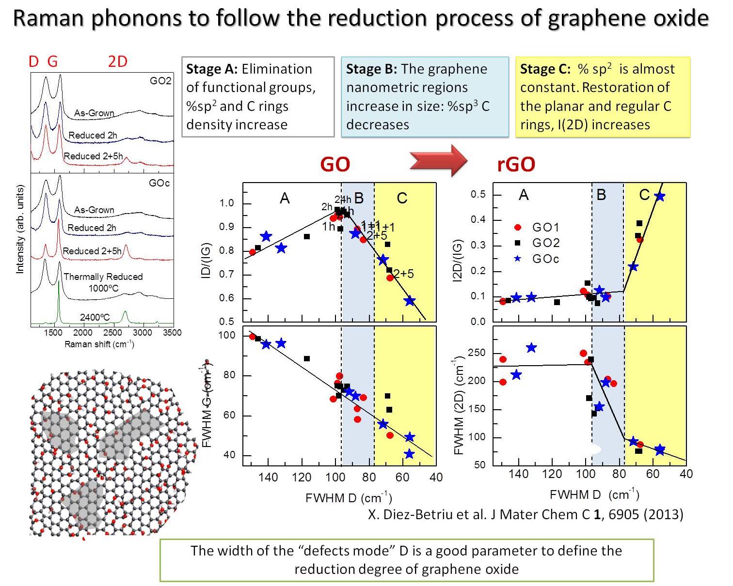
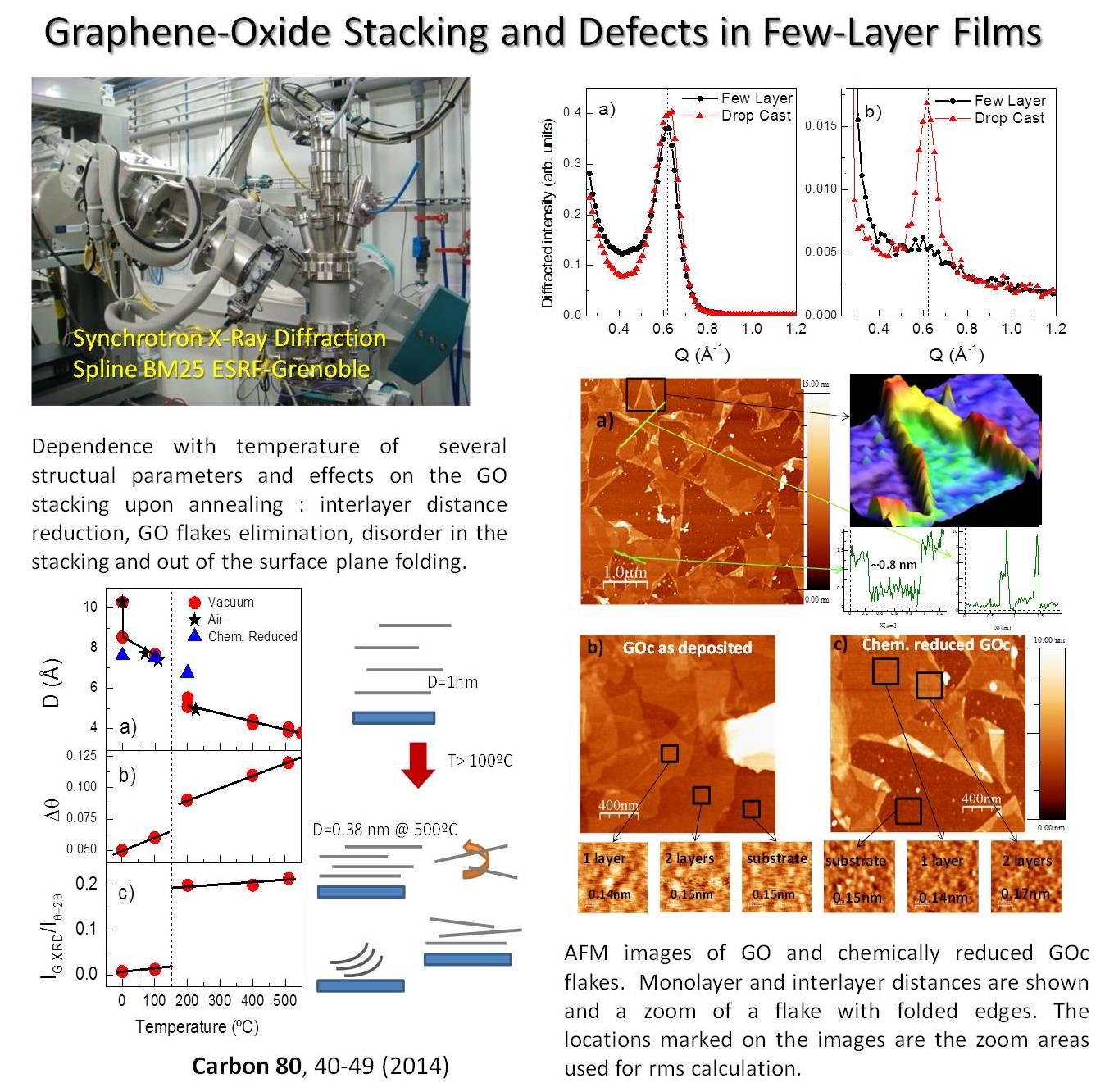
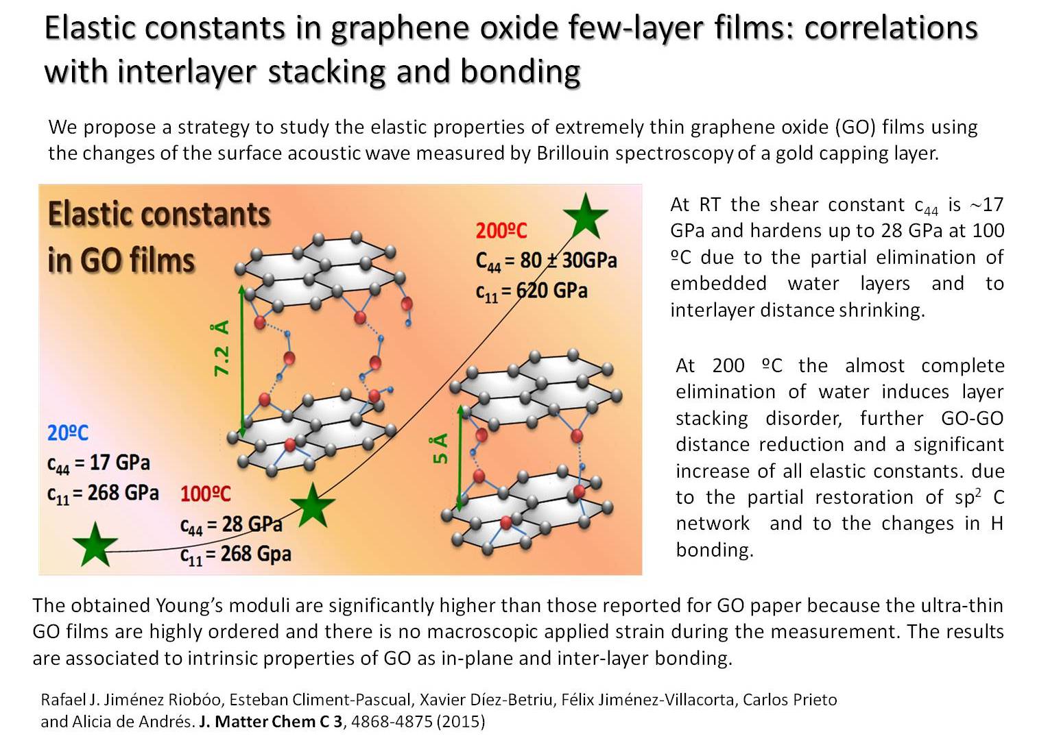