Scanning probe lithography is based on the spatial confinement of chemical reactions. This nanolithography is compatible with atmospheric pressure environments which could lead to low-cost approaches for making nanometer-scale devices.

a. Scheme of SPL. b. Classification of the SPL families
The chemistry involved in scanning probe lithography and thus the type of fabricated nanopatterns can be tuned by changing the reaction media, e.g, using organic vapors (fig 2a) or ozone-enriched atmosphere (fig 2b) or changing the substrate material, e.g, silicon (fig 2c) or MoS2 thin film (fig 2d).
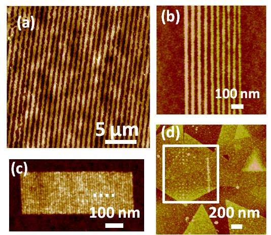
a. Octane SPL made parallel array of wires b. Silicon oxide patterns made by O- SPL in ozone c.Silicon oxide lines made by O-SPL d.MoO3 features patterned on a thin layer of MoS2
Relevant publications:
•R. Garcia, A. W. Knoll and E. Riedo, Nature Nanotechnology 9, 577 (2014)
•R. V. Martínez and R. García,Nano Letters 5, 1161 (2005)
•M. Calleja and R. García Applied Physics Letters 76, 3427 (2000)
•R. García, N.S. Losilla, J. Martínez, R.V. Martínez, F.J. Palomares, Y. Huttel, M. Calvaresi, and F. Zerbetto
Applied Physics Letters 96, 143110 (2010)
•F. M. Espinosa, Y. K. Ryu, K. Marinov, D. Dumcenco, A. Kis and R. García. Applied Physics Letters ,106, 103503 (2015)